RT9011
10
DS9011-09 July 2017www.richtek.com
For recommended operating conditions specification of
RT9011, the maximum junction temperature is 125°C. The
junction to ambient thermal resistance ( θ
JA
is layout
dependent ) for TSOT-23-6 is 220°C/W, WDFN-8L 2x2 is
165°C/W, WDFN-10L 3x3 is 108°C/W, WDFN-8L 3x3 is
108°C/W and WDFN-8L 1.6x1.6 is 175°C/W on the
standard JEDEC 51-3 single-layer thermal test board. The
maximum power dissipation at T
A
= 25°C can be calculated
by following formula :
P
D(MAX)
= ( 125°C − 25°C ) / (220°C/W) = 0.455W for
TSOT-23-6 packages
P
D(MAX)
= ( 125°C − 25°C ) / (165°C/W) = 0.606W for
WDFN-8L 2x2 packages
P
D(MAX)
= ( 125°C − 25°C ) / (108°C/W) = 0.926W for
WDFN-10L 3x3 packages
P
D(MAX)
= ( 125°C − 25°C ) / (108°C/W) = 0.926W for
WDFN-8L 3x3 packages
P
D(MAX)
= ( 125°C − 25°C ) / (175°C/W) = 0.571W for
WDFN-6L 1.6x1.6 packages
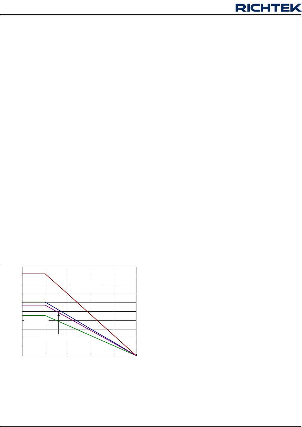
The maximum power dissipation depends on operating
ambient temperature for fixed T
J(MAX)
and thermal
resistance θ
JA
. For RT9011 packages, the Figure 3 of de-
rating curves allows the designer to see the effect of rising
ambient temperature on the maximum power allowed.
Figure 3. Derating Curves for RT9011 Packages
0
0.1
0.2
0.3
0.4
0.5
0.6
0.7
0.8
0.9
1
0 25 50 75 100 125
Ambient Temperature (°C)
Power Dissipation (W)
WDFN-8L 2x2
TSOT-23-6
WDFN-8L 3x3
WDFN-10L 3x3
Single Layer PCB
WDFN-6L 1.6x1.6

