RT9011
9
DS9011-09 July 2017 www.richtek.com
Applications Information
Like any low-dropout regulator, the external capacitors used
with the RT9011 must be carefully selected for regulator
stability and performance. Using a capacitor whose value
is > 1μF on the RT9011 input and the amount of capacitance
can be increased without limit. The input capacitor must
be located a distance of not more than 0.5 inch from the
input pin of the IC and returned to a clean analog ground.
Any good quality ceramic or tantalum can be used for this
capacitor. The capacitor with larger value and lower ESR
(equivalent series resistance) provides better PSRR and
line-transient response.
The output capacitor must meet both requirements for
minimum amount of capacitance and ESR in all LDOs
application. The RT9011 is designed specifically to work
with low ESR ceramic output capacitor in space-saving
and performance consideration. Using a ceramic capacitor
whose value is at least 1μF with ESR is > 20mΩ on the
RT9011 output ensures stability. The RT9011 still works
well with output capacitor of other types due to the wide
stable ESR range. Figure 1. shows the curves of allowable
ESR range as a function of load current for various output
capacitor values. Output capacitor of larger capacitance
can reduce noise and improve load transient response,
stability, and PSRR. The output capacitor should be located
not more than 0.5 inch from the VOUT pin of the RT9011
and returned to a clean analog ground.
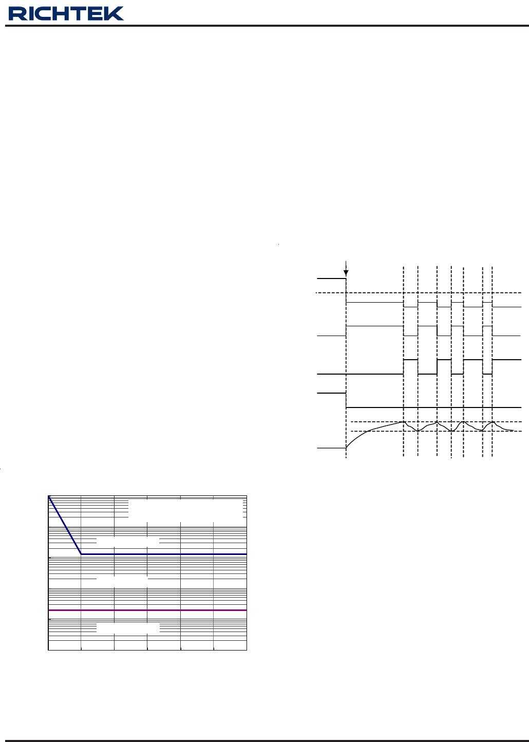
Figure 1. Stable Cout ESR Range
V
OUT
Short to GND
0.4V
V
OUT
I
OUT
TSD
OTP Trip Point
170 C
110 C
110 C
80 C
IC Temperature
Figure 2. Short Circuit Thermal Folded Back Protection
when Output Short Circuit Occurs (Patent)
Thermal Considerations
Thermal protection limits power dissipation in RT9011.
When the operation junction temperature exceeds 170°C,
the OTP circuit starts the thermal shutdown function and
turns the pass element off. The pass element turns on
again after the junction temperature cools by 40°C.
RT9011 lowers its OTP trip level from 170°C to 110°C
when output short circuit occurs (V
OUT
< 0.4V) as shown
in Figure 2. It limits IC case temperature under 100°C and
provides maximum safety to customer while output short
circuit occurring.
For continuous operation, do not exceed absolute
maximum operation junction temperature 125°C. The
power dissipation definition in device is :
P
D
= (V
IN
-V
OUT
) x I
OUT
+ V
IN
x I
Q
The maximum power dissipation depends on the thermal
resistance of IC package, PCB layout, the rate of
surroundings airflow and temperature difference between
junction to ambient. The maximum power dissipation can
be calculated by following formula :
P
D(MAX)
= ( T
J(MAX)
- T
A
) /θ
JA
Where T
J(MAX)
is the maximum operation junction
temperature, T
A
is the ambient temperature and the θ
JA
is
the junction to ambient thermal resistance.
Region of Stable C
OUT
ESR vs. Load Current
0.001
0.01
0.1
1
10
100
0 50 100 150 200 250 300
Load Current (mA)
Region of Stable C
OUT
ESR (Ω)
Region of Stable C
OUT
ESR (Ω)
Unstable Range
Stable Range
Simulation Verify
RT9011-FM, V
IN
= 5V
C
IN
= C
OUT1
= C
OUT2
= 1uF/X7R