RT9011
4
DS9011-09 July 2017www.richtek.com
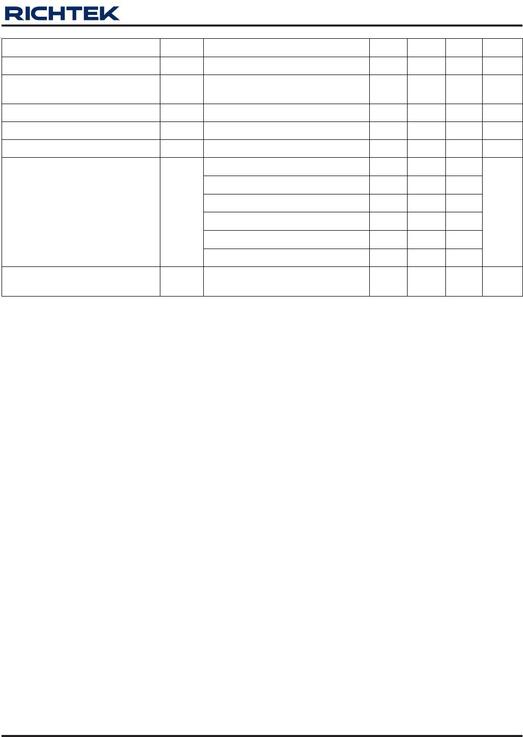
Electrical Characteristics
Parameter Symbol Test Conditions Min Typ Max Unit
Input Voltage
V
IN
= 2.5V to 5.5V
2.5 -- 5.5 V
Dropout Voltage (Note 5)
V
DROP
I
OUT
= 300mA
-- 240 330
mV
Output Voltage Range
V
OUT
1.2 -- 3.5 V
V
OUT
Accuracy
V
I
OUT
= 1mA to 300mA
3
-- +3 %
Line Regulation
V
LINE
V
IN
= (V
OUT
+ 0.3V) to 5.5V or
V
IN
> 2.5V, whichever is larger
-- -- 0.2 %/V
Load Regulation
V
LOAD
1mA < I
OUT
< 300mA
-- -- 0.6
%
Current Limit
R
LOAD
= 1
330 450 700 mA
Quiescent Current
I
Q
V
EN
> 1.5V
-- 58 80
A
Shutdown Current
I
Q_SD
V
EN
< 0.4V
-- -- 1
A
EN Threshold
V
IH
V
IN
= 2.5V to 5.5V, Power On
1.5 -- --
V
V
IL
V
IN
= 2.5V to 5.5V, Shutdown
-- -- 0.4
(V
IN
= V
OUT
+ 1V, V
EN
= V
IN
, C
IN
= C
OUT
= 1μF, T
A
= −40°C to 85°C, unless otherwise specified.)
To be continued
Recommended Operating Conditions (Note 4)
Supply Input Voltage ---------------------------------------------------------------------------------------------------- 2.5V to 5.5V
Enable Input Voltage ---------------------------------------------------------------------------------------------------- 0V to 5.5V
Junction Temperature Range ------------------------------------------------------------------------------------------ −40°C to 125°C
Ambient Temperature Range ------------------------------------------------------------------------------------------ −40°C to 85°C
Absolute Maximum Ratings (Note 1)
Supply Input Voltage ---------------------------------------------------------------------------------------------------- −0.3V to 7V
Other I/O Pin Voltages-------------------------------------------------------------------------------------------------- −0.3V to 7V
Power Dissipation, P
D
@ T
A
= 25°C
TSOT-23-6 ----------------------------------------------------------------------------------------------------------------- 0.455W
WDFN-8L 2x2 ------------------------------------------------------------------------------------------------------------- 0.606W
WDFN-10L 3x3 ----------------------------------------------------------------------------------------------------------- 0.926W
WDFN-8L 3x3 ------------------------------------------------------------------------------------------------------------- 0.926W
WDFN-6L 1.6x1.6 -------------------------------------------------------------------------------------------------------- 0.571W
Package Thermal Resistance (Note 2)
TSOT-23-6, θ
JA
----------------------------------------------------------------------------------------------------------- 220°C/W
WDFN-8L 2x2, θ
JA
------------------------------------------------------------------------------------------------------- 165°C/W
WDFN-10L 3x3, θ
JA
------------------------------------------------------------------------------------------------------ 108°C/W
WDFN-8L 3x3, θ
JA
------------------------------------------------------------------------------------------------------- 108°C/W
WDFN-6L 1.6x1.6, θ
JA
-------------------------------------------------------------------------------------------------- 175°C/W
Junction Temperature --------------------------------------------------------------------------------------------------- 150°C
Lead Temperature (Soldering, 10 sec.) ----------------------------------------------------------------------------- 260°C
Storage Temperature Range ------------------------------------------------------------------------------------------- −65°C to 150°C
ESD Susceptibility (Note 3)
HBM (Human Body Mode) --------------------------------------------------------------------------------------------- 2kV
MM (Machine Mode) ---------------------------------------------------------------------------------------------------- 200V