General Description
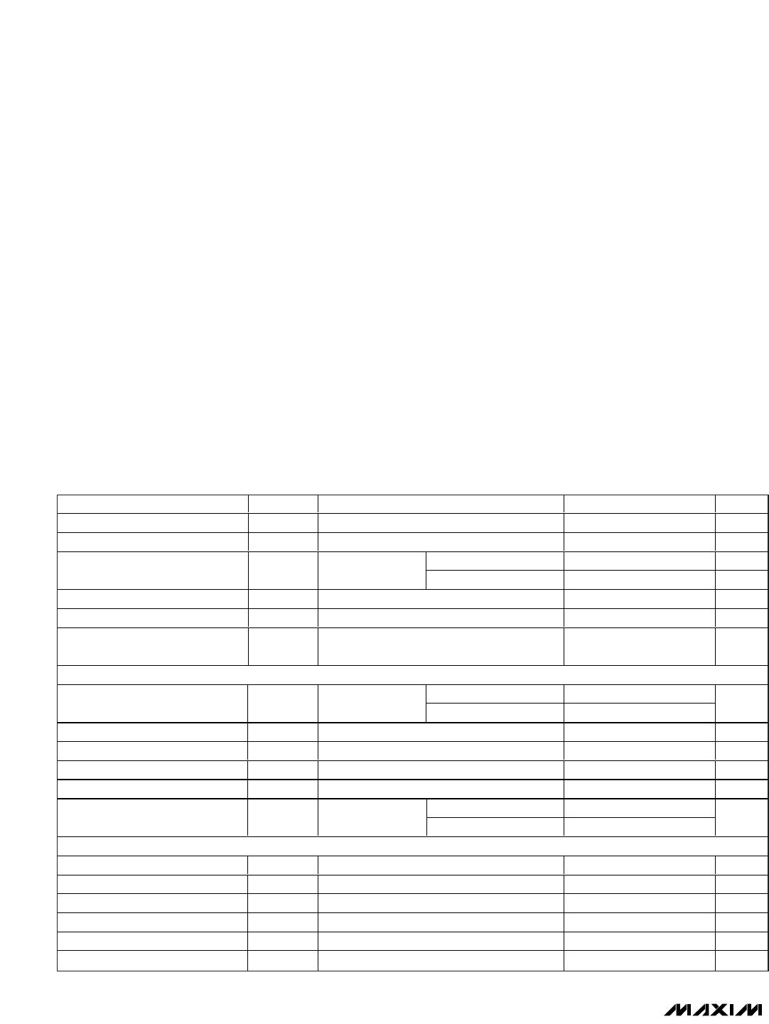
The MAX4885 integrates high-bandwidth analog
switches and level-translating buffers to implement a
complete 1:2 or 2:1 multiplexer for VGA signals. The
device provides switching for RGB, display data chan-
nel (DDC), and horizontal and vertical synchronization
(HSYNC, VSYNC) signals. A low-noise charge pump
with internal capacitors provides a boosted gate-drive
voltage to improve performance of the RGB switches.
In the 1:2 multiplexer mode, HSYNC/VSYNC inputs fea-
ture level-shifting buffers to support low-voltage CMOS
or standard TTL-compatible graphics controllers. In the
2:1 multiplexer mode, the output buffers for the
HSYNC/VSYNC inputs are disabled, allowing bidirec-
tional signaling. In both modes, DDC signals are volt-
age-clamped to an external voltage to provide level
translation and protection. The MAX4885 features a
5µA shutdown mode and is ESD protected to ±8kV
Human Body Model (HBM) on externally routed pins.
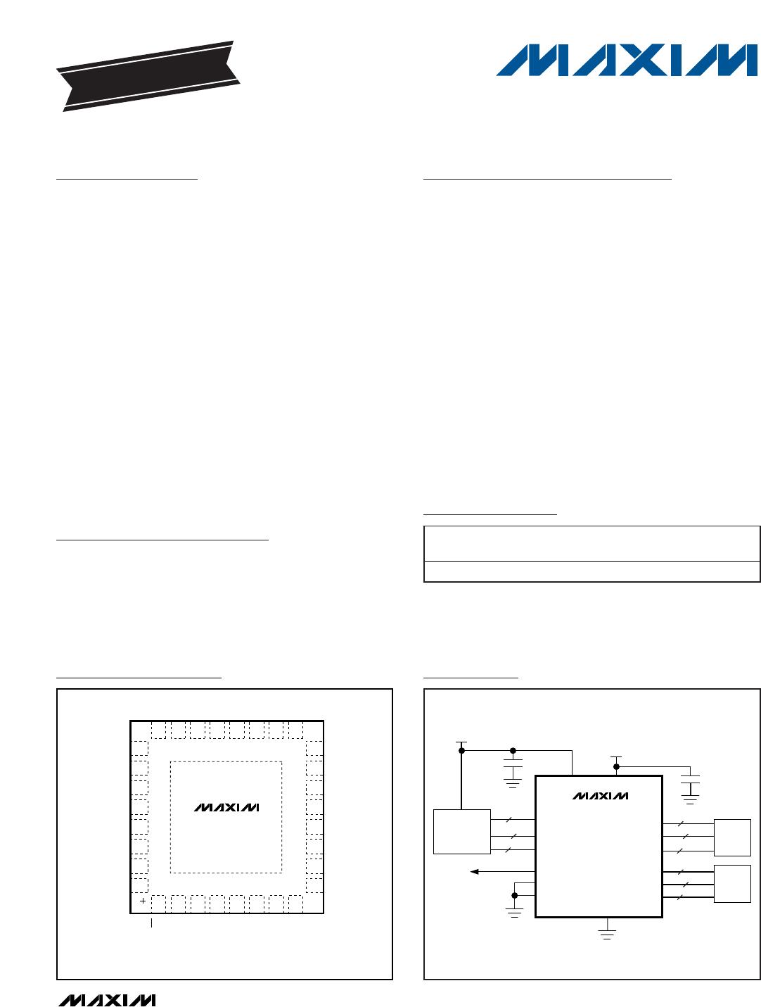
The MAX4885 is specified over the extended (-40°C to
+85°C) temperature range, and is available in the 32-
pin, 5mm x 5mm TQFN package.
Applications
Notebook Computers
Digital Projectors
Computer Monitors
Servers
KVM Switches
Features
+5V Single-Supply Operation
Programmable Voltage Clamp for Open-Drain
DDC Signals
Low 5Ω (typ) On-Resistance (R, G, B Signals)
Low 13pF (typ) On-Capacitance (R, G, B Signals)
Break-Before-Make Switching Protects Against
Circuit Shorts
±8kV HBM ESD Protection on Externally Routed
Pins
Low 300µA Supply Current (Lower than 1µA with
Charge Pump Disabled)
Space-Saving, Lead-Free, 32-Pin (5mm x 5mm)
TQFN Package
MAX4885
Complete VGA 1:2 or 2:1 Multiplexer
________________________________________________________________ Maxim Integrated Products 1
19-0554; Rev 0; 5/06
EVALUATION KIT
AVAILABLE
MAX4885
TQFN
TOP VIEW
29
30
28
27
12
11
13
R0
B0
H0
V0
DDCA0
14
QP
H1
V+
GND
B1
V2
H2
12
DDCA1
4567
2324 22 20 19 18
GND
V+
DDCB2
DDCA2
GND
V+
G0
V1
3
21
31
10
M
V
CL
32
9
SEL
EN
DDCB1
26
15
R2
R1
25
16
G2
DDCB0
B2
8
17
G1
*EXPOSED PADDLE CONNECTED TO GND
*EP
Pin Configuration
Ordering Information
GRAPHICS
CONTROLLER
V
CL
V+
GND
+3.3V
+5V
EN
SEL
R0, B0, G0
H0, V0
DDCA0, DDCB0
0.1μF
0.1μF
VGA
PORT 1
VGA
PORT 2
R2, G2, B2
H2, V2
DDCA2, DDCB2
2
3
2
2
3
2
R1, G1, B1
H1, V1
DDCA1, DDCB1
2
3
2
DOCKING
STATION
M
MAX4885
Typical Operating Circuit
PART
TEMP RANGE
PIN-PACKAGE
PKG
CODE
MAX4885ETJ+
-40°C to +85°C
32 TQFN-EP*
T3255-4
*EP = Exposed pad.
+Denotes lead-free package.
For pricing, delivery, and ordering information, please contact Maxim Direct at 1-888-629-4642,
or visit Maxim's website at www.maxim-ic.com.
MAX4885
Complete VGA 1:2 or 2:1 Multiplexer
2 _______________________________________________________________________________________
ABSOLUTE MAXIMUM RATINGS
Stresses beyond those listed under “Absolute Maximum Ratings” may cause permanent damage to the device. These are stress ratings only, and functional
operation of the device at these or any other conditions beyond those indicated in the operational sections of the specifications is not implied. Exposure to
absolute maximum rating conditions for extended periods may affect device reliability.
(All voltages referenced to GND.)
V
+
, V
CL
.....................................................................-0.3V to +6V
R_, G_, B_, DDCA_, DDCB_, SEL, M,
EN, QP (Note 1) ...........................................-0.3V to V+ + 0.3V
H_, V_ .......................................................................-0.3V to +6V
Continuous Current Through RGB Switches ....................±70mA
Continuous Current Through HV, DDC Switches…..........±50mA
Peak Current Through RGB Switches
(pulsed at 1ms, 10% duty cycle).................................±140mA
Peak Current Through HV, DDC Switches (pulsed at 1ms,
10% duty cycle)..............................................................±100mA
Continuous Power Dissipation (T
A
= +70°C)
32-Pin TQFN (derate 21.3mW/°C above +70°C) ........1702mW
Operating Temperature Range ...........................-40°C to +85°C
Storage Temperature Range .............................-65°C to +150°C
Junction Temperature......................................................+150°C
Lead Temperature (soldering, 10s) .................................+300°C
ELECTRICAL CHARACTERISTICS
(V+ = +5.0V ±10%, V
CL
= +3.3V ±10%, T
A
= T
MIN
to T
MAX
, QP = GND, unless otherwise noted. Typical values are at V+ = +5.0V,
V
CL
= +3.3V and T
A
= +25°C.)
SYMBOL
MIN
TYP
MAX
UNITS
V+ = +5.5V, all digital inputs to V+ or GND
I
CLSHDN
0V < V
IN
< +2.5V,
R
FLAT
(
ON
)
0.02 0.75
R_, G_, B_ = 0V,
+16
Note 1: Signals exceeding V+ or GND are clamped by internal diodes. Limit forward-diode current to maximum current rating.
MAX4885
Complete VGA 1:2 or 2:1 Multiplexer
_______________________________________________________________________________________ 3
SYMBOL
MIN
TYP
MAX
UNITS
R
ON
(
DDC
)
ELECTRICAL CHARACTERISTICS (continued)
(V+ = +5.0V ±10%, V
CL
= +3.3V ±10%, T
A
= T
MIN
to T
MAX
, QP = GND, unless otherwise noted. Typical values are at V+ = +5.0V,
V
CL
= +3.3V and T
A
= +25°C.)
SYMBOL
MIN TYP MAX
UNITS
350
350
0.85
200
AC ELECTRICAL CHARACTERISTICS
(V+ = +5.0V ±10%, V
CL
= +3.3V ±10%, T
A
= T
MIN
to T
MAX
, QP = GND. Typical values are at V+ = +5.0V, V
CL
= +3.3V and T
A
=
+25°C, unless otherwise noted.) (Note 2)

MAX4885ETJ+T

Mfr. #:
Manufacturer:
Maxim Integrated
Description:
Video Switch ICs Complete VGA 1:2 or 2:1 MUX
Lifecycle:
New from this manufacturer.
Delivery:
DHL FedEx Ups TNT EMS
Payment:
T/T Paypal Visa MoneyGram Western Union

Products related to this Datasheet