MAX4885
Complete VGA 1:2 or 2:1 Multiplexer
10 ______________________________________________________________________________________
standard VGA signals. The charge pump can be dis-
abled to eliminate charge-pump noise; however, RGB
switch performance is slightly degraded. Connect QP
to ground for normal operation.
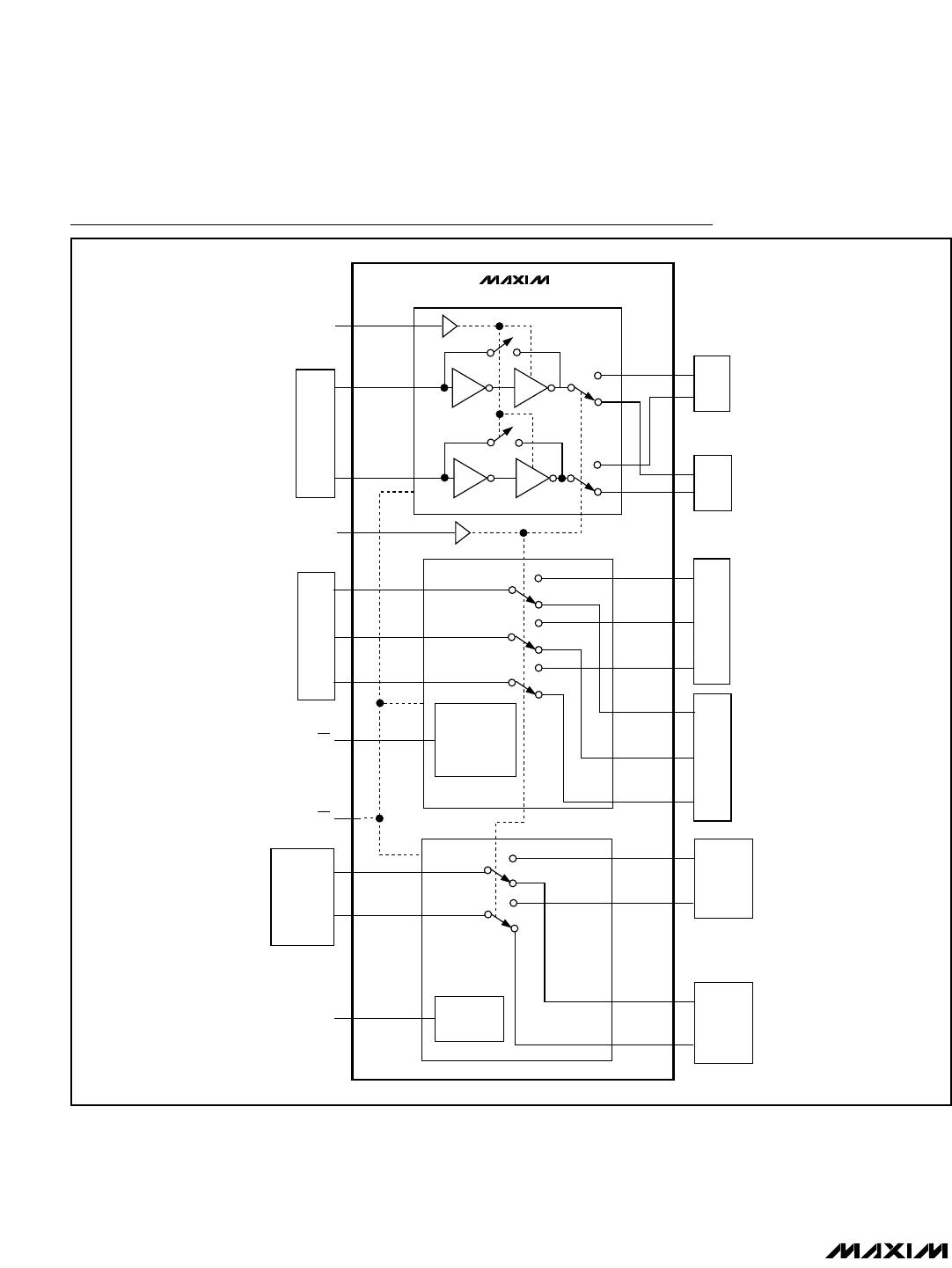
Horizontal/Vertical Sync Multiplexer
1:2 Multiplexer Mode
The MAX4885 provides two modes of operation for the
HSYNC and VSYNC signals. In 1:2 mode (M = 0), the
HSYNC/VSYNC inputs are buffered to provide level shift-
ing and drive capability to meet the VESA specification.
2:1 Multiplexer Mode
In 2:1 mode (M = 1), the HSYNC/VSYNC output buffers
are disabled, and switches pass signals directly. The
HSYNC and VSYNC switches/buffers are identical, and
either input can be used to route HSYNC and
VSYNC signals.
Display Data Channel Multiplexer
The MAX4885 provides two voltage-clamped switches
to route DDC signals (see Table 3). Each switch
clamps signals to a diode drop less than the voltage
applied on V
CL
. Supply +3.3V on V
CL
to provide volt-
age clamping for VESA I
2
C-compatible signals. If volt-
age clamping is not required, connect V
CL
to V+. The
DDCA and DDCB switches are identical, and each
switch can be used to route either DDC signal.
ESD Protection
As with all Maxim devices, ESD-protection structures
are incorporated on all pins to protect against electro-
static discharges encountered during handling and
assembly. Additionally, the MAX4885 is protected to
±8kV on RGB, HSYNC, VSYNC, and DDC switches by
the Human Body Model (HBM). For optimum ESD per-
formance, bypass each V+ pin to ground with a 0.1µF
or larger ceramic capacitor.
Human Body Model (HBM)
Several ESD testing standards exist for measuring the
robustness of ESD structures. The ESD protection of
the MAX4885 is characterized with the Human Body
Model. Figure 5 shows the model used to simulate an
ESD event resulting from contact with the human body.
The model consists of a 100pF storage capacitor that is
charged to a high voltage, then discharged through a
1.5kΩ resistor. Figure 6 shows the current waveform
when the storage capacitor is discharged into a low
impedance.
ESD Test Conditions
ESD performance depends on a variety of conditions.
Please contact Maxim for a reliability report document-
ing test setup, methodology, and results.
Applications Information
1:2 Multiplexer for Low-Voltage Graphics
Controllers
The MAX4885 provides the level shifting necessary to
drive two standard VGA ports from a graphics con-
troller as low as +2.2V. In 1:2 mode, internal buffers
drive the HSYNC and VSYNC signals to VGA standard
TTL levels. The DDC multiplexer provides level shifting
by clamping signals to a diode drop less than V
CL
(see
the Typical Operating Circuit). Connect V
CL
to +3.3V
for normal operation, or to V+ to disable voltage clamp-
ing for DDC signals.