Connectivity Test Mode
Connectivity test (CT) mode for the x16 TwinDie single rank (SR) device is the same as
two mono x8 devices connected in parallel. The mapping is restated for clarity.
Minimum Terms Definition for Logic Equations
The test input and output pins are related by the following equations, where INV de-
notes a logical inversion operation and XOR a logical exclusive OR operation:
MT0 = XOR (A1, A6, PAR)
MT1 = XOR (A8, ALERT_n, A9)
MT2 = XOR (A2, A5, A13)
MT3 = XOR (A0, A7, A11)
MT4 = XOR (CK_c, ODT, CAS_n/A15)
MT5 = XOR (CKE, RAS_n/A16, A10/AP)
MT6 = XOR (ACT_n, A4, BA1)
MT7L = XOR (BG1, LDM_n/LDBI_n, CK_t)
MT7U = XOR (BG1, UDM_n/UDBI_n, CK_t)
MT8 = XOR (WE_n/A14, A12 / BC, BA0)
MT9 = XOR (BG0, A3, RESET_n and TEN)
Logic Equations for a x16 TwinDie, SR Device
Byte 0
Byte 1
LDQ0 = MT0 UDQ0 = MT0
LDQ1 = MT1 UDQ1 = MT1
LDQ2 = MT2 UDQ2 = MT2
LDQ3 = MT3 UDQ3 = MT3
LDQ4 = MT4 UDQ4 = MT4
LDQ5 = MT5 UDQ5 = MT5
LDQ6 = MT6 UDQ6 = MT6
LDQ7 = MT7L UDQ7 = MT7U
LDQS_t = MT8 UDQS_t = MT8
LDQS_c = MT9 UDQS_c = MT9
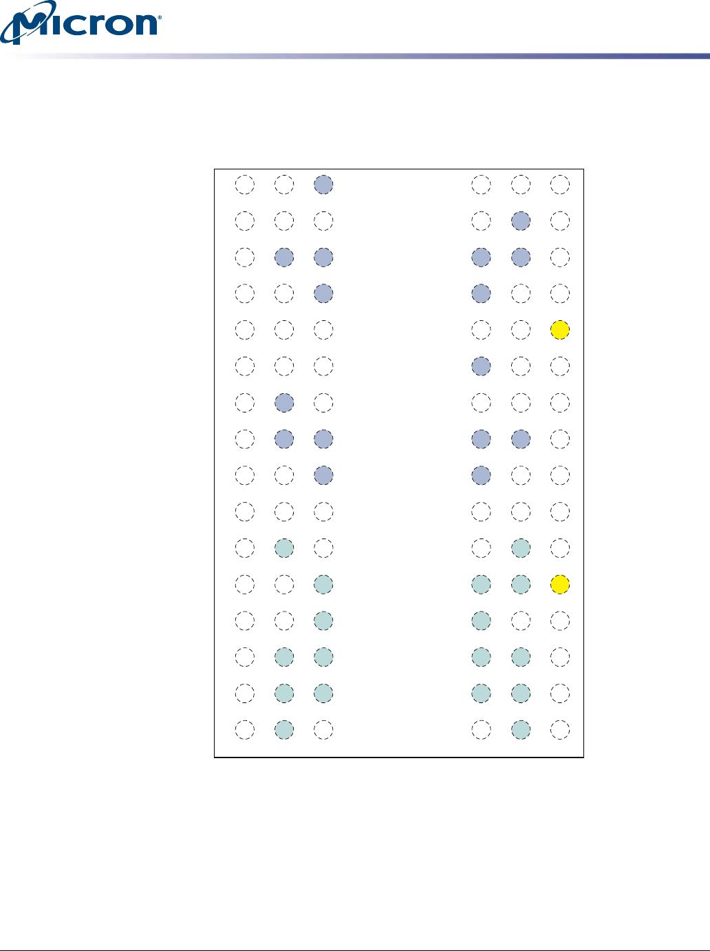
x16 TwinDie, SR Internal Connections
The figure below shows the internal connections of the x16 TwinDie, SR. The diagram
shows why byte 0 and byte 1 outputs have the same logic equations except LDQ7 and
UDQ7; they are different because the DM_n/DBI_n pins are not common for each byte.
16Gb: x16 TwinDie Single Rank DDR4 SDRAM
Connectivity Test Mode
CCMTD-1725822587-9947
16gb_x16_1cs_TwinDie.pdf - Rev. G 06/18 EN
6
Micron Technology, Inc. reserves the right to change products or specifications without notice.
© 2015 Micron Technology, Inc. All rights reserved.