IL300-EF-X007T

IL300
www.vishay.com
Vishay Semiconductors
Rev. 1.8, 02-Jun-14
1
Document Number: 83622
For technical questions, contact: optocoupleranswers@vishay.com
THIS DOCUMENT IS SUBJECT TO CHANGE WITHOUT NOTICE. THE PRODUCTS DESCRIBED HEREIN AND THIS DOCUMENT
ARE SUBJECT TO SPECIFIC DISCLAIMERS, SET FORTH AT www.vishay.com/doc?91000
Linear Optocoupler, High Gain Stability, Wide Bandwidth
DESCRIPTION
The IL300 linear optocoupler consists of an AlGaAs IRLED
irradiating an isolated feedback and an output PIN
photodiode in a bifurcated arrangement. The feedback
photodiode captures a percentage of the LEDs flux and
generates a control signal (I
P1
) that can be used to servo the
LED drive current. This technique compensates for the
LED’s non-linear, time, and temperature characteristics.
The output PIN photodiode produces an output signal (I
P2
)
that is linearly related to the servo optical flux created by the
LED.
The time and temperature stability of the input-output
coupler gain (K3) is insured by using matched PIN
photodiodes that accurately track the output flux of the LED.
FEATURES
Couples AC and DC signals
0.01 % servo linearity
Wide bandwidth, > 200 kHz
High gain stability, ± 0.005 %/°C typically
Low input-output capacitance
Low power consumption, < 15 mW
Isolation test voltage, 5300 V
RMS
, 1 s
Internal insulation distance, > 0.4 mm
Material categorization: for definitions of compliance
please see www.vishay.com/doc?99912
APPLICATIONS
Power supply feedback voltage/current
Medical sensor isolation
Audio signal interfacing
Isolated process control transducers
Digital telephone isolation
AGENCY APPROVALS
UL file no. E52744, system code H
DIN EN 60747-5-5 (VDE 0884-5) available with option 1
•BSI
•FIMKO
Note
(1)
Also available in tubes, do not put “T” on the end.
A
C
NC
NC
C
A
A
C
1
2
3
4
8
7
6
5
K2
K1
i179026_2
V
DE
i179026
ORDERING INFORMATION
I L300-DEFG-X0##T
PART NUMBER K3 BIN PACKAGE OPTION TAPE
AND
REEL
AGENCY
CERTIFIED/
PACKAGE
K3 BIN
UL, cUL,
BSI, FIMKO
0.557 to 1.618 0.765 to 1.181 0.851 to 1.181 0.765 to 0.955 0.851 to 1.061 0.945 to 1.181 0.851 to 0.955 0.945 to 1.061
DIP-8 IL300 IL300-DEFG - - IL300-EF - IL300-E IL300-F
DIP-8, 400 mil,
option 6
IL300-X006 IL300-DEFG-X006 - - IL300-EF-X006 IL300-FG-X006 IL300-E-X006 IL300-F-X006
SMD-8, option 7 IL300-X007T
(1)
IL300-DEFG-X007T
(1)
IL300-EFG-X007 IL300-DE-X007T IL300-EF-X007T
(1)
- IL300-E-X007T IL300-F-X007
SMD-8, option 9 IL300-X009T
(1)
IL300-DEFG-X009T
(1)
- - IL300-EF-X009T
(1)
- - IL300-F-X009T
(1)
VDE, UL
,
BSI, FIMKO
0.557 to 1.618 0.765 to 1.181 0.851 to 1.181 0.765 to 0.955 0.851 to 1.061 0.945 to 1.181 0.851 to 0.955 0.945 to 1.061
DIP-8 IL300-X001 IL300-DEFG-X001 - - IL300-EF-X001 - IL300-E-X001 IL300-F-X001
DIP-8, 400 mil,
option 6
IL300-X016 IL300-DEFG-X016 - - IL300-EF-X016 - - IL300-F-X016
SMD-8, option 7 IL300-X017 IL300-DEFG-X017T
(1)
- - IL300-EF-X017T
(1)
- IL300-E-X017T IL300-F-X017T
(1)
SMD-8, option 9 - - - - - - - IL300-F-X019T
(1)
> 0.1 mm
10.16 mm
> 0.7 mm
7.62 mm
DIP-8
Option 7
Option 6
Option 9
IL300
www.vishay.com
Vishay Semiconductors
Rev. 1.8, 02-Jun-14
2
Document Number: 83622
For technical questions, contact: optocoupleranswers@vishay.com
THIS DOCUMENT IS SUBJECT TO CHANGE WITHOUT NOTICE. THE PRODUCTS DESCRIBED HEREIN AND THIS DOCUMENT
ARE SUBJECT TO SPECIFIC DISCLAIMERS, SET FORTH AT www.vishay.com/doc?91000
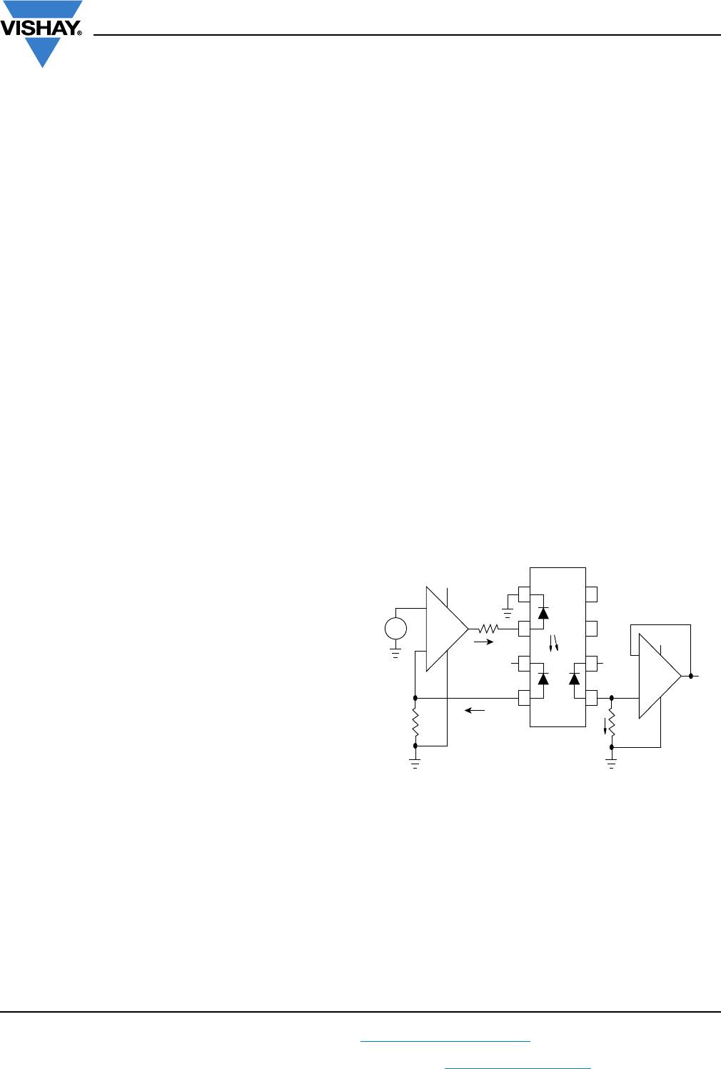
OPERATION DESCRIPTION
A typical application circuit (figure 1) uses an operational
amplifier at the circuit input to drive the LED. The feedback
photodiode sources current to R1 connected to the inverting
input of U1. The photocurrent, I
P1
, will be of a magnitude to
satisfy the relationship of (I
P1
= V
IN
/R1).
The magnitude of this current is directly proportional to the
feedback transfer gain (K1) times the LED drive current
(V
IN
/R1 = K1 x I
F
). The op-amp will supply LED current to
force sufficient photocurrent to keep the node voltage (Vb)
equal to Va.
The output photodiode is connected to a non-inverting
voltage follower amplifier. The photodiode load resistor, R2,
performs the current to voltage conversion. The output
amplifier voltage is the product of the output forward gain
(K2) times the LED current and photodiode load,
R2 (V
O
= I
F
x K2 x R2).
Therefore, the overall transfer gain (V
O
/V
IN
) becomes the
ratio of the product of the output forward gain (K2) times the
photodiode load resistor (R2) to the product of the feedback
transfer gain (K1) times the input resistor (R1). This reduces
to
V
O
/V
IN
= (K2 x R2)/(K1 x R1).
The overall transfer gain is completely independent of the
LED forward current. The IL300 transfer gain (K3) is
expressed as the ratio of the output gain (K2) to the
feedback gain (K1). This shows that the circuit gain
becomes the product of the IL300 transfer gain times the
ratio of the output to input resistors
V
O
/V
IN
= K3 (R2/R1).
K1-SERVO GAIN
The ratio of the input photodiode current (I
P1
) to the LED
current (I
F
) i.e., K1 = I
P1
/I
F
.
K2-FORWARD GAIN
The ratio of the output photodiode current (I
P2
) to the LED
current (I
F
), i.e., K2 = I
P2
/I
F
.
K3-TRANSFER GAIN
The transfer gain is the ratio of the forward gain to the servo
gain, i.e., K3 = K2/K1.
K3-TRANSFER FAIN LINEARITY
The percent deviation of the transfer gain, as a function of
LED or temperature from a specific transfer gain at a fixed
LED current and temperature.
PHOTODIODE
A silicon diode operating as a current source. The output
current is proportional to the incident optical flux supplied
by the LED emitter. The diode is operated in the photovoltaic
or photoconductive mode. In the photovoltaic mode the
diode functions as a current source in parallel with a forward
biased silicon diode.
The magnitude of the output current and voltage is
dependent upon the load resistor and the incident LED
optical flux. When operated in the photoconductive mode
the diode is connected to a bias supply which reverse
biases the silicon diode. The magnitude of the output
current is directly proportional to the LED incident optical
flux.
LED (LIGHT EMITTING DIODE)
An infrared emitter constructed of AlGaAs that emits at
890 nm operates efficiently with drive current from 500 μA to
40 mA. Best linearity can be obtained at drive currents
between 5 mA to 20 mA. Its output flux typically changes by
-0.5 %/°C over the above operational current range.
APPLICATION CIRCUIT
Fig. 1 - Typical Application Circuit
8
7
6
5
K1
1
2
3
4
K2
R1
R2
IL300
Vb
Va
+
-
U1
V
in
lp1
-
U2
+
lp2
V
out
V
CC
V
CC
V
CC
V
CC
I
F
V
C
+
R3
IL300
www.vishay.com
Vishay Semiconductors
Rev. 1.8, 02-Jun-14
3
Document Number: 83622
For technical questions, contact: optocoupleranswers@vishay.com
THIS DOCUMENT IS SUBJECT TO CHANGE WITHOUT NOTICE. THE PRODUCTS DESCRIBED HEREIN AND THIS DOCUMENT
ARE SUBJECT TO SPECIFIC DISCLAIMERS, SET FORTH AT www.vishay.com/doc?91000
Note
Stresses in excess of the absolute maximum ratings can cause permanent damage to the device. Functional operation of the device is not
implied at these or any other conditions in excess of those given in the operational sections of this document. Exposure to absolute
maximum ratings for extended periods of the time can adversely affect reliability.
ABSOLUTE MAXIMUM RATINGS (T
amb
= 25 °C, unless otherwise specified)
PARAMETER TEST CONDITION SYMBOL VALUE UNIT
INPUT
Power dissipation P
diss
160 mW
Derate linearly from 25 °C 2.13 mW/°C
Forward current I
F
60 mA
Surge current (pulse width < 10 μs) I
PK
250 mA
Reverse voltage V
R
5V
Thermal resistance R
th
470 K/W
Junction temperature T
j
100 °C
OUTPUT
Power dissipation P
diss
50 mW
Derate linearly from 25 °C 0.65 mW/°C
Reverse voltage V
R
50 V
Thermal resistance R
th
1500 K/W
Junction temperature T
j
100 °C
COUPLER
Total package dissipation at 25 °C P
tot
210 mW
Derate linearly from 25 °C 2.8 mW/°C
Storage temperature T
stg
-55 to +150 °C
Operating temperature T
amb
-55 to +100 °C
Isolation test voltage V
ISO
> 5300 V
RMS
Isolation resistance
V
IO
= 500 V, T
amb
= 25 °C R
IO
> 10
12
V
IO
= 500 V, T
amb
= 100 °C R
IO
> 10
11
ELECTRICAL CHARACTERISTICS (T
amb
= 25 °C, unless otherwise specified)
PARAMETER TEST CONDITION SYMBOL MIN. TYP. MAX. UNIT
INPUT (LED EMITTER)
Forward voltage I
F
= 10 mA V
F
1.25 1.50 V
V
F
temperature coefficient V
F
/°C -2.2 mV/°C
Reverse current V
R
= 5 V I
R
A
Junction capacitance V
F
= 0 V, f = 1 MHz C
j
15 pF
Dynamic resistance I
F
= 10 mA V
F
/I
F
6
OUTPUT
Dark current V
det
= -15 V, I
F
= 0 A I
D
125nA
Open circuit voltage I
F
= 10 mA V
D
500 mV
Short circuit current I
F
= 10 mA I
SC
70 μA
Junction capacitance V
F
= 0 V, f = 1 MHz C
j
12 pF
Noise equivalent power V
det
= 15 V NEP 4 x 10
-14
W/Hz
COUPLER
Input-output capacitance V
F
= 0 V, f = 1 MHz 1 pF
K1, servo gain (I
P1
/I
F
)I
F
= 10 mA, V
det
= -15 V K1 0.0050 0.007 0.011
Servo current
(1)(2)
I
F
= 10 mA, V
det
= -15 V I
P1
70 μA
K2, forward gain (I
P2
/I
F
)I
F
= 10 mA, V
det
= -15 V K2 0.0036 0.007 0.011
Forward current I
F
= 10 mA, V
det
= -15 V I
P2
70 μA
K3, transfer gain (K2/K1)
(1)(2)
I
F
= 10 mA, V
det
= -15 V K3 0.56 1 1.65 K2/K1

IL300-EF-X007T

Mfr. #:
Manufacturer:
Vishay Semiconductors
Description:
High Linearity Optocouplers Single Linear, High Gain, Wide Bandwidth
Lifecycle:
New from this manufacturer.
Delivery:
DHL FedEx Ups TNT EMS
Payment:
T/T Paypal Visa MoneyGram Western Union