IL300-EF-X007T

IL300
www.vishay.com
Vishay Semiconductors
Rev. 1.8, 02-Jun-14
4
Document Number: 83622
For technical questions, contact: optocoupleranswers@vishay.com
THIS DOCUMENT IS SUBJECT TO CHANGE WITHOUT NOTICE. THE PRODUCTS DESCRIBED HEREIN AND THIS DOCUMENT
ARE SUBJECT TO SPECIFIC DISCLAIMERS, SET FORTH AT www.vishay.com/doc?91000
Notes
Minimum and maximum values were tested requierements. Typical values are characteristics of the device and are the result of engineering
evaluation. Typical values are for information only and are not part of the testing requirements.
(1)
Bin sorting:
K3 (transfer gain) is sorted into bins that are ± 6 % , as follows:
Bin A = 0.557 to 0.626
Bin B = 0.620 to 0.696
Bin C = 0.690 to 0.773
Bin D = 0.765 to 0.859
Bin E = 0.851 to 0.955
Bin F = 0.945 to 1.061
Bin G = 1.051 to 1.181
Bin H = 1.169 to 1.311
Bin I = 1.297 to 1.456
Bin J = 1.442 to 1.618
K3 = K2/K1. K3 is tested at I
F
= 10 mA, V
det
= -15 V.
(2)
Bin categories: All IL300s are sorted into a K3 bin, indicated by an alpha character that is marked on the part. The bins range from “A”
through “J”.
The IL300 is shipped in tubes of 50 each. Each tube contains only one category of K3. The category of the parts in the tube is marked on
the tube label as well as on each individual part.
(3)
Category options: standard IL300 orders will be shipped from the categories that are available at the time of the order. Any of the ten
categories may be shipped. For customers requiring a narrower selection of bins, the bins can be grouped together as follows:
IL300-DEFG: order this part number to receive categories D, E, F, G only.
IL300-EF: order this part number to receive categories E, F only.
IL300-E: order this part number to receive category E only.
COUPLER
Transfer gain stability I
F
= 10 mA, V
det
= -15 V K3/T
A
± 0.005 ± 0.15 %/°C
Transfer gain linearity
I
F
= 1 mA to 10 mA K3 ± 0.25 %
I
F
= 1 mA to 10 mA,
T
amb
= 0 °C to 75 °C
± 0.5 %
PHOTOCONDUCTIVE OPERATION
Frequency response
I
Fq
= 10 mA, MOD = ± 4 mA,
R
L
= 50
BW (-3 db) 200 kHz
Phase response at 200 kHz V
det
= -15 V -45 Deg.
SWITCHING CHARACTERISTICS
PARAMETER TEST CONDITION SYMBOL MIN. TYP. MAX. UNIT
Switching time I
F
= 2 mA, I
Fq
= 10 mA
t
r
s
t
f
s
Rise time t
r
1.75 μs
Fall time t
f
1.75 μs
COMMON MODE TRANSIENT IMMUNITY
PARAMETER TEST CONDITION SYMBOL MIN. TYP. MAX. UNIT
Common mode capacitance V
F
= 0 V, f = 1 MHz C
CM
0.5 pF
Common mode rejection ratio f = 60 Hz, R
L
= 2.2 k CMRR 130 dB
ELECTRICAL CHARACTERISTICS (T
amb
= 25 °C, unless otherwise specified)
PARAMETER TEST CONDITION SYMBOL MIN. TYP. MAX. UNIT
IL300
www.vishay.com
Vishay Semiconductors
Rev. 1.8, 02-Jun-14
5
Document Number: 83622
For technical questions, contact: optocoupleranswers@vishay.com
THIS DOCUMENT IS SUBJECT TO CHANGE WITHOUT NOTICE. THE PRODUCTS DESCRIBED HEREIN AND THIS DOCUMENT
ARE SUBJECT TO SPECIFIC DISCLAIMERS, SET FORTH AT www.vishay.com/doc?91000
TYPICAL CHARACTERISTICS (T
amb
= 25 °C, unless otherwise specified)
Fig. 2 - LED Forward Current vs. Forward Voltage
Fig. 3 - Servo Photocurrent vs. LED Current and Temperature
Fig. 4 - Normalized Servo Photocurrent vs.
LED Current and Temperature
Fig. 5 - Servo Gain vs. LED Current and Temperature
Fig. 6 - Normalized Transfer Gain vs.
LED Current and Temperature
Fig. 7 - Amplitude Response vs. Frequency
iil300_02
1.41.31.21.1
0
5
10
15
20
25
30
35
V
F
- LED Forward Voltage (V)
I
F
- LED Current (mA)
1.0
iil300_04
0 °C
25 °C
50 °C
75 °C
0.1 1 10 100
300
250
200
150
100
50
0
I
F
- LED Current (mA)
I
P1
- Servo Photocurrent (µA)
V
D
= - 15 V
iil300_06
010152025
3.0
2.5
2.0
1.5
1.0
0.5
0.0
I
F
- LED Current (mA)
Normalized Photocurrent
Normalized to: I
P1
at
I
F
= 10 mA
T
A
= 25 °C
V
D
= - 15 V
0 °C
25 °C
50 °C
75 °C
5
I
F
- L ED Current (mA)
0.1 1 10 100
0
K1- Ser vo Gain - I
P1
/I
F
0.010
0.008
0.006
0.004
0.002
25°
50°
75°
100°
17754
iil300_11
010152025
1.010
1.005
1.000
0.995
0.990
I
F
- LED Current (mA)
K3 - Transfer Gain - (K2/K1)
0 °C
25 °C
50 °C
75 °C
Normalized to:
I
F
= 10 mA
T
A
= 25 °C
5
iil300_12
10
4
10
5
10
6
5
0
- 5
- 10
- 15
- 20
F - Frequency (Hz)
Amplitude Response (dB)
R
L
= 1 kΩ
I
F
= 10 mA, Mod = ± 2.0 Ma (peak)
R
L
= 10 kΩ
IL300
www.vishay.com
Vishay Semiconductors
Rev. 1.8, 02-Jun-14
6
Document Number: 83622
For technical questions, contact: optocoupleranswers@vishay.com
THIS DOCUMENT IS SUBJECT TO CHANGE WITHOUT NOTICE. THE PRODUCTS DESCRIBED HEREIN AND THIS DOCUMENT
ARE SUBJECT TO SPECIFIC DISCLAIMERS, SET FORTH AT www.vishay.com/doc?91000
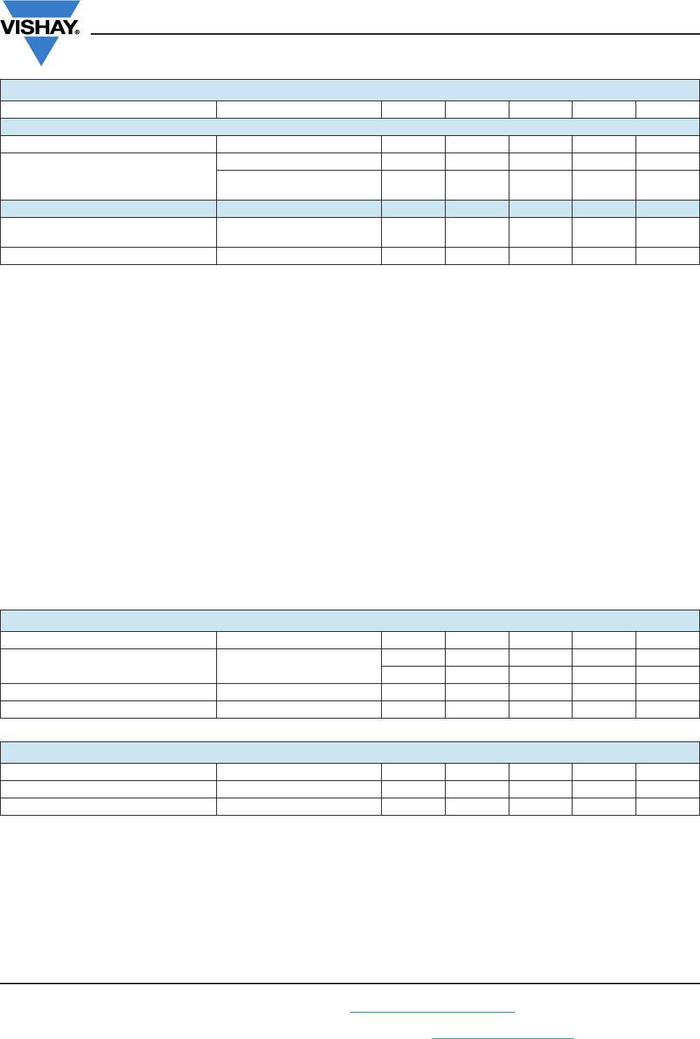
Fig. 8 - Amplitude and Phase Response vs. Frequency
Fig. 9 - Common-Mode Rejection
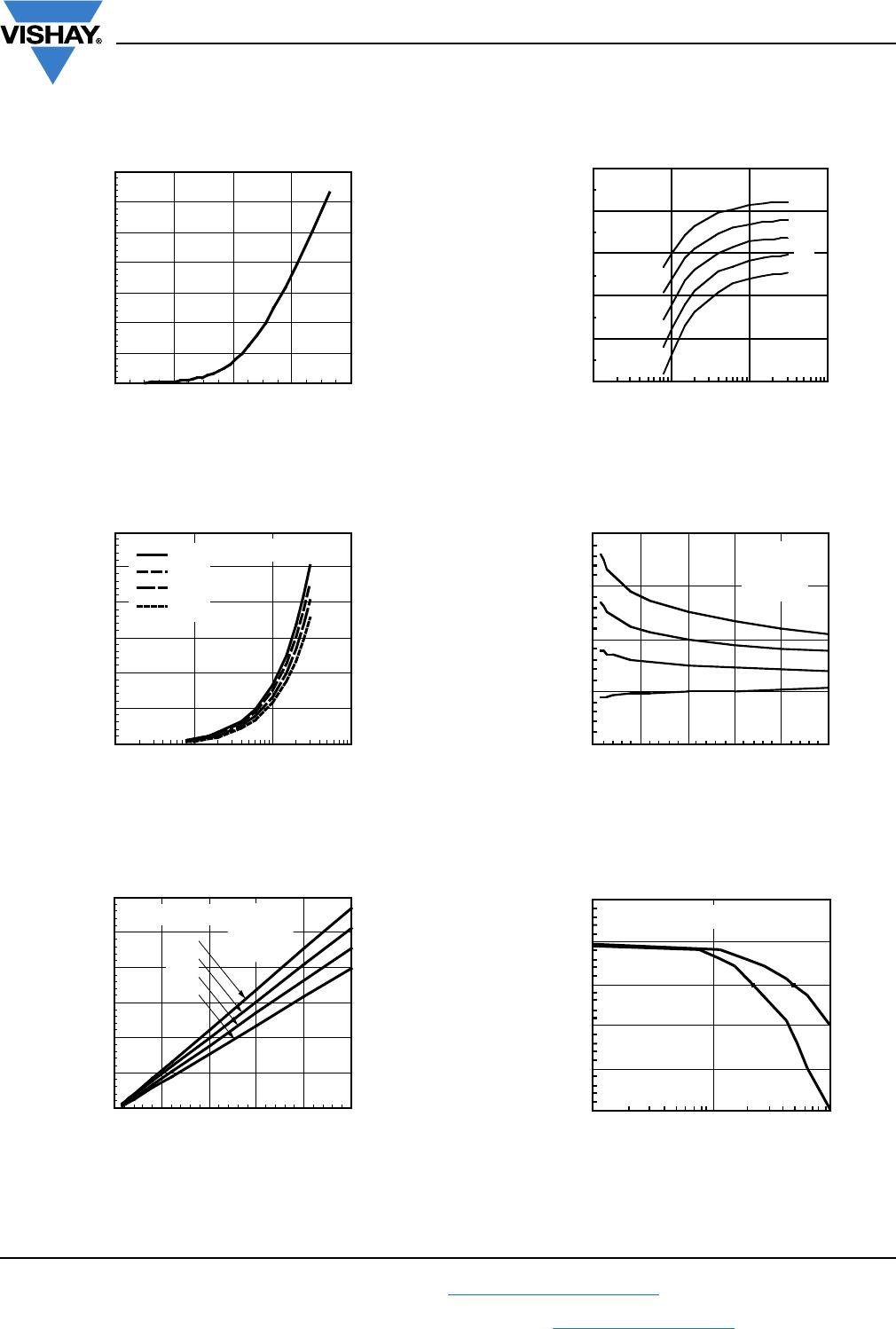
Fig. 10 - Photodiode Junction Capacitance vs.
Reverse Voltage
APPLICATION CONSIDERATIONS
In applications such as monitoring the output voltage from a
line powered switch mode power supply, measuring
bioelectric signals, interfacing to industrial transducers, or
making floating current measurements, a galvanically
isolated, DC coupled interface is often essential. The IL300
can be used to construct an amplifier that will meet these
needs.
The IL300 eliminates the problems of gain nonlinearity and
drift induced by time and temperature, by monitoring LED
output flux.
A pin photodiode on the input side is optically coupled to the
LED and produces a current directly proportional to flux
falling on it. This photocurrent, when coupled to an amplifier,
provides the servo signal that controls the LED drive current.
The LED flux is also coupled to an output PIN photodiode.
The output photodiode current can be directly or amplified
to satisfy the needs of succeeding circuits.
ISOLATED FEEDBACK AMPLIFIER
The IL300 was designed to be the central element of DC
coupled isolation amplifiers. Designing the IL300 into an
amplifier that provides a feedback control signal for a line
powered switch mode power is quite simple, as the
following example will illustrate.
See figure 12 for the basic structure of the switch mode
supply using the Infineon TDA4918 push-pull switched
power supply control cChip. Line isolation are provided by
the high frequency transformer. The voltage monitor
isolation will be provided by the IL300.
The isolated amplifier provides the PWM control signal
which is derived from the output supply voltage. Figure 13
more closely shows the basic function of the amplifier.
The control amplifier consists of a voltage divider and a
non-inverting unity gain stage. The TDA4918 data sheet
indicates that an input to the control amplifier is a high
quality operational amplifier that typically requires a + 3 V
signal. Given this information, the amplifier circuit topology
shown in figure 14 is selected.
The power supply voltage is scaled by R1 and R2 so that
there is + 3 V at the non-inverting input (V
a
) of U1. This
voltage is offset by the voltage developed by photocurrent
flowing through R3. This photocurrent is developed by the
optical flux created by current flowing through the LED.
Thus as the scaled monitor voltage (V
a
) varies it will cause a
change in the LED current necessary to satisfy the
differential voltage needed across R3 at the inverting input.
The first step in the design procedure is to select the value
of R3 given the LED quiescent current (I
Fq
) and the servo
gain (K1). For this design, I
Fq
= 12 mA. Figure 4 shows the
servo photocurrent at I
Fq
is found to be 100 mA. With this
data R3 can be calculated.
iil300_13
dB
Phase
Ø - Phase Response (°)
10
3
10
4
10
5
10
6
10
7
5
0
- 5
- 10
- 15
- 20
45
0
- 45
- 90
- 135
- 180
F - Frequency (Hz)
Amplitude Response (dB)
I
Fq
= 10 mA
Mod = ± 4.0 mA
T
A
= 25 °C
R
L
= 50 Ω
iil300_14
- 130
- 120
- 110
- 100
- 90
- 80
- 70
- 60
F - Frequency (Hz)
CMRR - Rejection Ratio (dB)
10
6
10
1
10
2
10
3
10
4
10
5
R3
V
b
I
PI
------
3 V
100 μA
------------------
30 k== =

IL300-EF-X007T

Mfr. #:
Manufacturer:
Vishay Semiconductors
Description:
High Linearity Optocouplers Single Linear, High Gain, Wide Bandwidth
Lifecycle:
New from this manufacturer.
Delivery:
DHL FedEx Ups TNT EMS
Payment:
T/T Paypal Visa MoneyGram Western Union