Precision CMOS, Single-Supply, Rail-to-Rail,
Input/Output Wideband Operational Amplifiers
AD8601/AD8602/AD8604
Rev. G
Information furnished by Analog Devices is believed to be accurate and reliable. However, no
responsibility is assumed by Analog Devices for its use, nor for any infringements of patents or other
rights of third parties that may result from its use. Specifications subject to change without notice. No
license is granted by implication or otherwise under any patent or patent rights of Analog Devices.
Trademarks and registered trademarks are the property of their respective owners.
One Technology Way, P.O. Box 9106, Norwood, MA 02062-9106, U.S.A.
Tel: 781.329.4700 www.analog.com
Fax: 781.461.3113 ©2000–2011 Analog Devices, Inc. All rights reserved.
FEATURES
Low offset voltage: 500 μV maximum
Single-supply operation: 2.7 V to 5.5 V
Low supply current: 750 μA/Amplifier
Wide bandwidth: 8 MHz
Slew rate: 5 V/μs
Low distortion
No phase reversal
Low input currents
Unity-gain stable
Qualified for automotive applications
APPLICATIONS
Current sensing
Barcode scanners
PA controls
Battery-powered instrumentation
Multipole filters
Sensors
ASIC input or output amplifiers
Audio
GENERAL DESCRIPTION
The AD8601, AD8602, and AD8604 are single, dual, and quad
rail-to-rail, input and output, single-supply amplifiers featuring
very low offset voltage and wide signal bandwidth. These amplifiers
use a new, patented trimming technique that achieves superior
performance without laser trimming. All are fully specified to
operate on a 3 V to 5 V single supply.
The combination of low offsets, very low input bias currents,
and high speed make these amplifiers useful in a wide variety
of applications. Filters, integrators, diode amplifiers, shunt
current sensors, and high impedance sensors all benefit from
the combination of performance features. Audio and other ac
applications benefit from the wide bandwidth and low distortion.
For the most cost-sensitive applications, the D grades offer this
ac performance with lower dc precision at a lower price point.
Applications for these amplifiers include audio amplification for
portable devices, portable phone headsets, bar code scanners,
portable instruments, cellular PA controls, and multipole filters.
The ability to swing rail-to-rail at both the input and output
enables designers to buffer CMOS ADCs, DACs, ASICs, and
other wide output swing devices in single-supply systems.
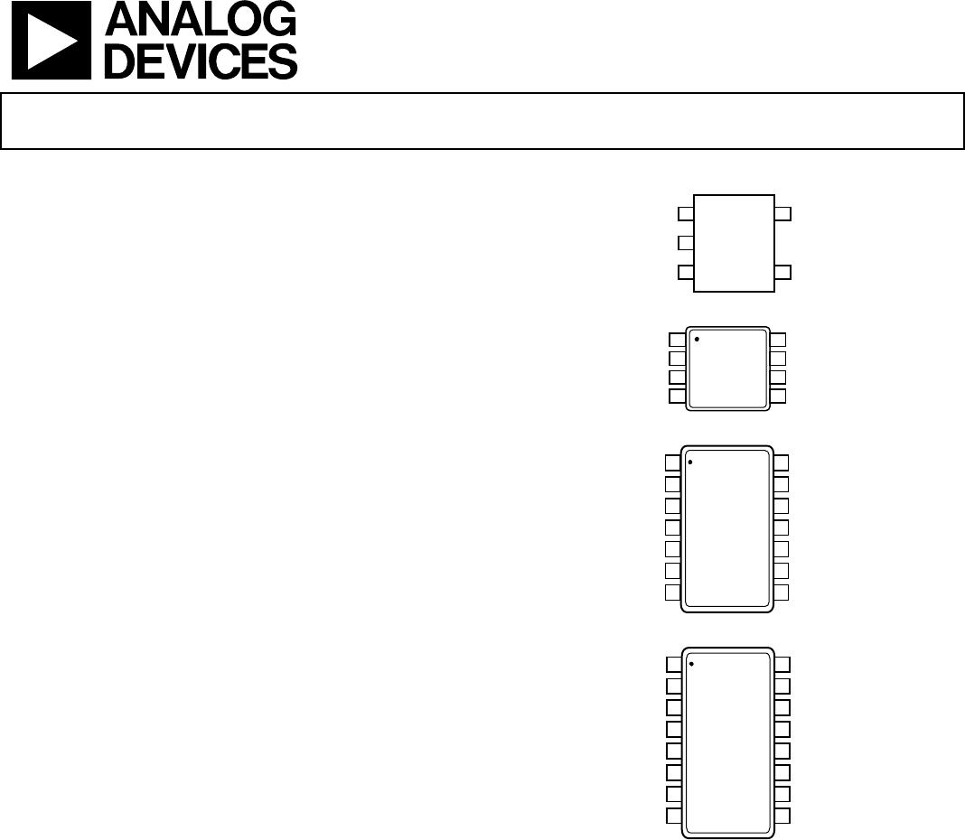
PIN CONFIGURATIONS
01525-001
OUT A
1
V–
2
+IN
3
V+
5
–IN
4
AD8601
TOP VIEW
(Not to Scale)
Figure 1. 5-Lead SOT-23 (RJ Suffix)
OUT A
1
–IN A
2
+IN A
3
V–
4
V+
8
OUT B
7
–IN B
6
+IN B
5
AD8602
TOP VIEW
(Not to Scale)
01525-002
Figure 2. 8-Lead MSOP (RM Suffix) and 8-Lead SOIC (R-Suffix)
01525-003
1
2
3
4
5
6
7
AD8604
–IN A
+IN A
V+
OUT B
–IN B
+IN B
OUT A
14
13
12
11
10
9
8
–IN D
+IN D
V–
OUT C
–IN C
+IN C
OUT D
TOP VIEW
(Not to Scale)
Figure 3. 14-Lead TSSOP (RU Suffix) and 14-Lead SOIC (R Suffix)
1
2
3
4
5
6
7
8
16
15
14
13
12
11
10
9
–IN A
+IN A
V+
OUT B
–IN B
+IN B
OUT A
–IN D
+IN D
V–
OUT C
NC NC
NC = NO CONNECT
–IN C
+IN C
OUT D
TOP VIEW
(Not to Scale)
AD8604
01525-004
Figure 4. 16-Lead Shrink Small Outline QSOP (RQ Suffix)
The AD8601, AD8602, and AD8604 are specified over the
extended industrial (−40°C to +125°C) temperature range. The
AD8601, single, is available in a tiny, 5-lead SOT-23 package. The
AD8602, dual, is available in 8-lead MSOP and 8-lead, narrow
SOIC surface-mount packages. The AD8604, quad, is available
in 14-lead TSSOP, 14-lead SOIC, and 16-lead QSOP packages.
See the Ordering Guide for automotive grades.
AD8601/AD8602/AD8604
Rev. G | Page 2 of 24
TABLE OF CONTENTS
Features .............................................................................................. 1
Applications....................................................................................... 1
General Description......................................................................... 1
Pin Configurations ........................................................................... 1
Revision History ............................................................................... 2
Specifications..................................................................................... 3
Electrical Characteristics............................................................. 3
Absolute Maximum Ratings............................................................ 5
Thermal Resistance ...................................................................... 5
ESD Caution.................................................................................. 5
Typical Performance Characteristics ............................................. 6
Theory of Operation ...................................................................... 15
Rail-to-Rail Input Stage ............................................................. 15
Input Overvoltage Protection................................................... 16
Overdrive Recovery ................................................................... 16
Power-On Time .......................................................................... 16
Using the AD8602 in High Source Impedance
Applications ................................................................................ 16
High Side and Low Side, Precision Current Monitoring ...... 16
Using the AD8601 in Single-Supply, Mixed Signal
Applications ................................................................................ 17
PC100 Compliance for Computer Audio Applications ........ 17
SPICE Model............................................................................... 18
Outline Dimensions....................................................................... 19
Ordering Guide .......................................................................... 22
Automotive Products ................................................................. 22
REVISION HISTORY
1/11—Rev. F to Rev. G
Changes to Ordering Guide .......................................................... 22
Change to Automotive Products Section .................................... 22
5/10—Rev. E to Rev. F
Changes to Features Section and General Description
Section................................................................................................ 1
Changes to Ordering Guide .......................................................... 22
Added Automotive Products Section .......................................... 22
2/10—Rev. D to Rev. E
Add 16-Lead QSOP............................................................Universal
Changes to Table 3 and Table 4....................................................... 5
Updated Outline Dimensions....................................................... 19
Changes to Ordering Guide .......................................................... 22
11/03—Rev. C to Rev. D
Changes to Features ..........................................................................1
Changes to Ordering Guide.............................................................4
3/03—Rev. B to Rev. C
Changes to Features ..........................................................................1
3/03—Rev. A to Rev. B
Change to Features ............................................................................1
Change to Functional Block Diagrams...........................................1
Change to TPC 39 .......................................................................... 11
Changes to Figures 4 and 5 ........................................................... 14
Changes to Equations 2 and 3................................................. 14, 15
Updated Outline Dimensions....................................................... 16
AD8601/AD8602/AD8604
Rev. G | Page 3 of 24
SPECIFICATIONS
ELECTRICAL CHARACTERISTICS
V
S
= 3 V, V
CM
= V
S
/2, T
A
= 25°C, unless otherwise noted.
Table 1.
A Grade D Grade
Parameter Symbol Conditions Min Typ Max Min Typ Max Unit
INPUT CHARACTERISTICS
Offset Voltage (AD8601/AD8602) V
OS
0 V ≤ V
CM
≤ 1.3 V 80 500 1100 6000 μV
−40°C T
A
≤ +85°C 700 7000 μV
−40°C T
A
≤ +125°C 1100 7000 μV
0 V ≤ V
CM
≤ 3 V
1
350 750 1300 6000 μV
−40°C T
A
≤ +85°C 1800 7000 μV
−40°C T
A
≤ +125°C 2100 7000 μV
Offset Voltage (AD8604) V
OS
V
CM
= 0 V to 1.3 V 80 600 1100 6000 μV
−40°C T
A
≤ +85°C 800 7000 μV
−40°C T
A
≤ +125°C 1600 7000 μV
V
CM
= 0 V to 3.0 V
1
350 800 1300 6000 μV
−40°C T
A
≤ +85°C 2200 7000 μV
−40°C T
A
≤ +125°C 2400 7000 μV
Input Bias Current I
B
0.2 60 0.2 200 pA
−40°C T
A
≤ +85°C 25 100 25 200 pA
−40°C T
A
≤ +125°C 150 1000 150 1000 pA
Input Offset Current I
OS
0.1 30 0.1 100 pA
−40°C T
A
≤ +85°C 50 100 pA
−40°C T
A
≤ +125°C 500 500 pA
Input Voltage Range 0 3 0 3 V
Common-Mode Rejection Ratio CMRR V
CM
= 0 V to 3 V 68 83 52 65 dB
Large Signal Voltage Gain A
VO
V
O
= 0.5 V to 2.5 V,
R
L
= 2 kΩ, V
CM
= 0 V
30 100 20 60 V/mV
Offset Voltage Drift ΔV
OS
/ΔT 2 2 μV/°C
OUTPUT CHARACTERISTICS
Output Voltage High V
OH
I
L
= 1.0 mA 2.92 2.95 2.92 2.95 V
–40°C T
A
+125°C 2.88 2.88 V
Output Voltage Low V
OL
I
L
= 1.0 mA 20 35 20 35 mV
−40°C T
A
+125°C 50 50 mV
Output Current I
OUT
±30 ±30 mA
Closed-Loop Output Impedance Z
OUT
f = 1 MHz, A
V
= 1 12 12 Ω
POWER SUPPLY
Power Supply Rejection Ratio PSRR V
S
= 2.7 V to 5.5 V 67 80 56 72 dB
Supply Current/Amplifier I
SY
V
O
= 0 V 680 1000 680 1000 μA
−40°C T
A
≤ +125°C 1300 1300 μA
DYNAMIC PERFORMANCE
Slew Rate SR R
L
= 2 kΩ 5.2 5.2 V/μs
Settling Time t
S
To 0.01% <0.5 <0.5 μs
Gain Bandwidth Product GBP 8.2 8.2 MHz
Phase Margin Φo 50 50 Degrees
NOISE PERFORMANCE
Voltage Noise Density e
n
f = 1 kHz 33 33 nV/√Hz
f = 10 kHz 18 18 nV/√Hz
Current Noise Density i
n
0.05 0.05 pA/√Hz
1
For V
CM
between 1.3 V and 1.8 V, V
OS
may exceed specified value.

AD8601ARTZ-REEL7

Mfr. #:
Manufacturer:
Analog Devices Inc.
Description:
Precision Amplifiers RRIO SGL w/ Low Offset VTG
Lifecycle:
New from this manufacturer.
Delivery:
DHL FedEx Ups TNT EMS
Payment:
T/T Paypal Visa MoneyGram Western Union