AD8601/AD8602/AD8604
Rev. G | Page 15 of 24
THEORY OF OPERATION
The AD8601/AD8602/AD8604 family of amplifiers are rail-to-rail
input and output, precision CMOS amplifiers that operate from
2.7 V to 5.0 V of the power supply voltage. These amplifiers use
Analog Devices, Inc., DigiTrim® technology to achieve a higher
degree of precision than available from most CMOS amplifiers.
DigiTrim technology is a method of trimming the offset voltage
of the amplifier after it has been assembled. The advantage in post-
package trimming lies in the fact that it corrects any offset voltages
due to the mechanical stresses of assembly. This technology is
scalable and used with every package option, including the 5-lead
SOT-23, providing lower offset voltages than previously achieved in
these small packages.
The DigiTrim process is completed at the factory and does not
add additional pins to the amplifier. All AD860x amplifiers are
available in standard op amp pinouts, making DigiTrim completely
transparent to the user. The AD860x can be used in any precision
op amp application.
The input stage of the amplifier is a true rail-to-rail architecture,
allowing the input common-mode voltage range of the op amp
to extend to both positive and negative supply rails. The voltage
swing of the output stage is also rail-to-rail and is achieved by
using an NMOS and PMOS transistor pair connected in a
common-source configuration. The maximum output voltage
swing is proportional to the output current, and larger currents
limit how close the output voltage can get to the supply rail,
which is a characteristic of all rail-to-rail output amplifiers.
With 1 mA of output current, the output voltage can reach
within 20 mV of the positive rail and within 15 mV of the
negative rail. At light loads of >100 kΩ, the output swings
within ~1 mV of the supplies.
The open-loop gain of the AD860x is 80 dB, typical, with a load
of 2 kΩ. Because of the rail-to-rail output configuration, the gain
of the output stage and the open-loop gain of the amplifier are
dependent on the load resistance. Open-loop gain decreases with
smaller load resistances. Again, this is a characteristic inherent
to all rail-to-rail output amplifiers.
RAIL-TO-RAIL INPUT STAGE
The input common-mode voltage range of the AD860x extends
to both the positive and negative supply voltages. This maximizes
the usable voltage range of the amplifier, an important feature
for single-supply and low voltage applications. This rail-to-rail
input range is achieved by using two input differential pairs, one
NMOS and one PMOS, placed in parallel. The NMOS pair is
active at the upper end of the common-mode voltage range, and
the PMOS pair is active at the lower end.
The NMOS and PMOS input stages are separately trimmed using
DigiTrim to minimize the offset voltage in both differential pairs.
Both NMOS and PMOS input differential pairs are active in a
500 mV transition region, when the input common-mode voltage
is between approximately 1.5 V and 1 V below the positive supply
voltage. The input offset voltage shifts slightly in this transition
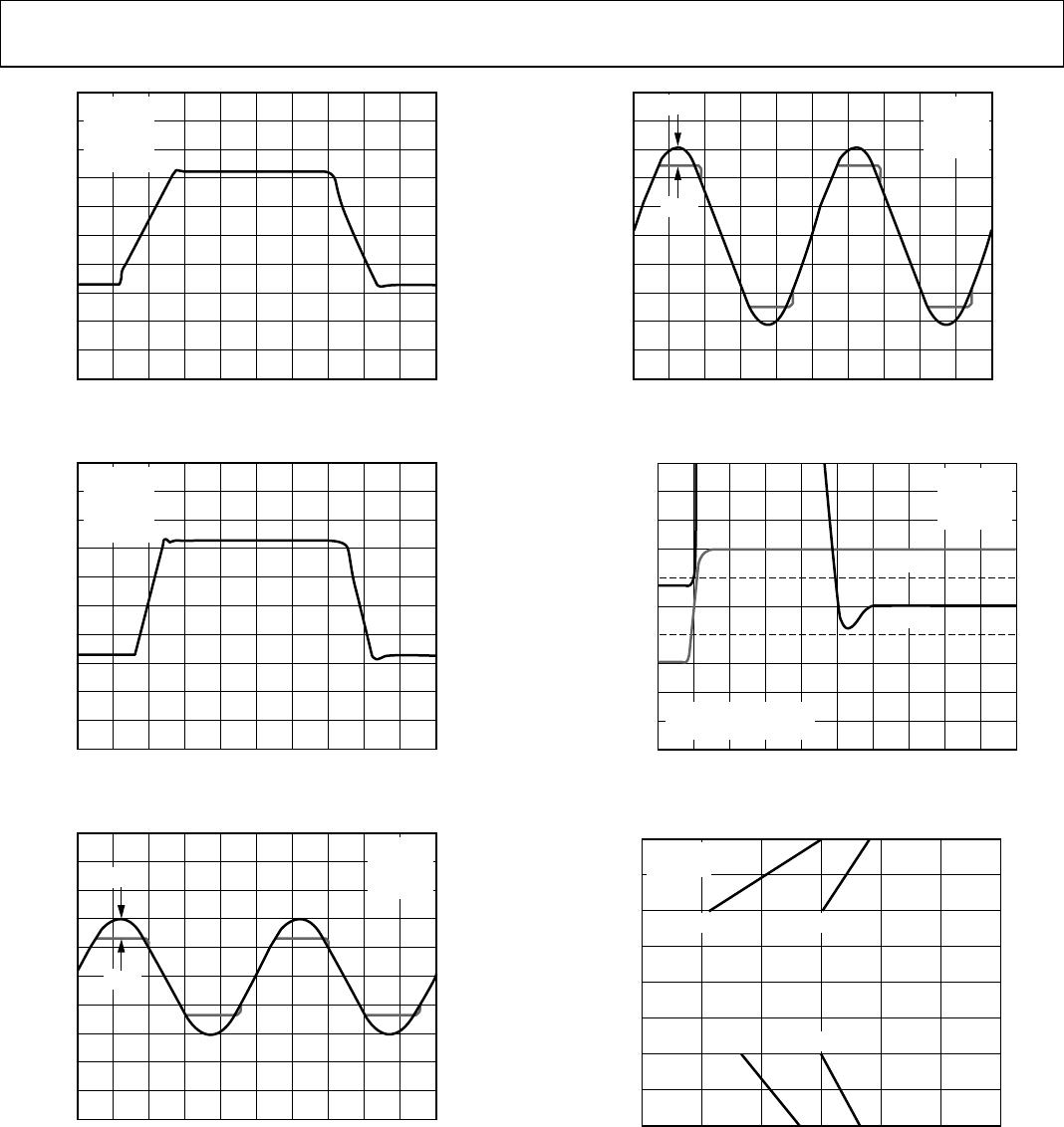
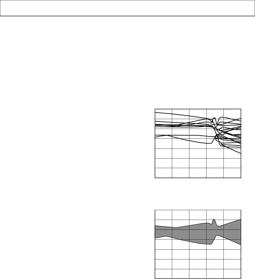
region, as shown in Figure 9 and Figure 10 .The common-mode
rejection ratio is also slightly lower when the input common-
mode voltage is within this transition band. Compared to the
Burr-Brown OPA2340UR rail-to-rail input amplifier, shown in
Figure 54, the AD860x, shown in Figure 55, exhibits lower
offset voltage shift across the entire input common-mode
range, including the transition region.
0.7
0.4
0.1
–0.2
–0.5
–0.8
–1.1
–1.4
012345
V
CM
(V)
V
OS
(mV)
01525-054
Figure 54. Burr-Brown OPA2340UR Input Offset Voltage vs.
Common-Mode Voltage, 24 SOIC Units @ 25°C
0.7
0.4
0.1
–0.2
–0.5
–0.8
–1.1
–1.4
012345
V
CM
(V)
V
OS
(mV)
01525-055
Figure 55. AD8602AR Input Offset Voltage vs. Common-Mode Voltage,
300 SOIC Units @ 25°C