Expand menu
Hello, Sign in
My Account
0
Cart
Home
Products
Sensors
Semiconductors
Passive Components
Connectors
Power
Electromechanical
Optoelectronics
Circuit Protection
Integrated Circuits - ICs
Main Products
Manufacturers
Blog
Services
About OMO
About Us
Contact Us
Check Stock
NCV8402ADDR2G
P1-P3
P4-P6
P7-P9
P10-P11
NCV8402D, NCV8402AD
www
.onsemi.com
4
4.
Fault conditions are viewed as beyond the normal operating range of the part.
5.
Not subject to production testing.
NCV8402D, NCV8402AD
www
.onsemi.com
5
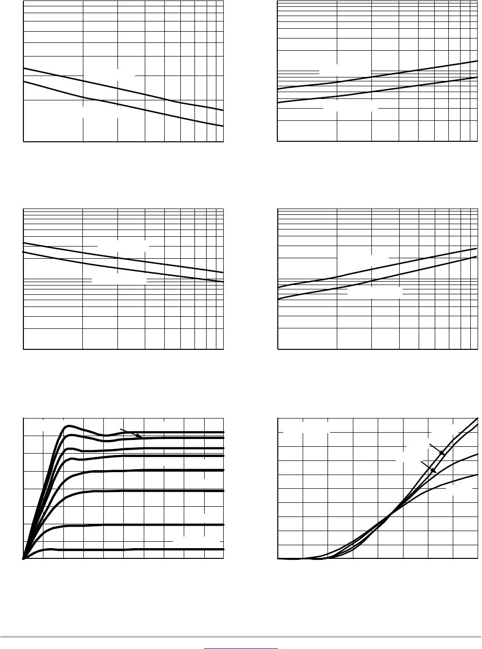
TYPICAL PERFORMANCE CUR
VES
1
10
10
100
Figure 2. Single Pulse Maximum Switch−off
Current vs. Load Inductance
L (mH)
I
L(max)
(A)
T
Jstart
= 25
°
C
T
Jstart
= 150
°
C
10
100
1000
10
1
00
Figure 3. Single Pulse Maximum Switching
Energy vs. Load Inductance
L (mH)
E
max
(mJ)
T
Jstart
= 25
°
C
T
Jstart
= 150
°
C
0.1
1
10
11
0
Figure 4. Single Pulse Maximum Inductive
Switch−off Current vs. Time in Clamp
TIME IN CLAMP (ms)
I
L(max)
(A)
T
Jstart
= 25
°
C
T
Jstart
= 150
°
C
10
100
1000
11
0
Figure 5. Single Pulse Maximum Inductive
Switching Energy vs. Time in Clamp
TIME IN CLAMP (ms)
E
max
(mJ)
T
Jstart
= 25
°
C
T
Jstart
= 150
°
C
V
DS
(V)
I
D
(A)
Figure 6. On−state Output Characteristics
V
GS
= 2.5 V
3 V
4 V
5 V
6 V
8 V
10 V
T
A
= 25
°
C
0
1
2
3
4
5
1234
5
V
DS
= 10 V
25
°
C
100
°
C
150
°
C
−40
°
C
I
D
(A)
V
GS
(V)
Figure 7. T
ransfer Characteristics
0
1
2
3
4
5
6
7
8
012
345
3.5 V
NCV8402D, NCV8402AD
www
.onsemi.com
6
TYPICAL PERFORMANCE CUR
VES
0
100
200
300
400
4567
89
1
0
Figure 8. R
DS(on)
vs. Gate−Source V
oltage
V
GS
(V)
R
DS(on)
(m
W
)
150
°
C, I
D
= 0.5
A
150
°
C, I
D
= 1.7
A
100
°
C, I
D
= 0.5
A
100
°
C, I
D
= 1.7
A
25
°
C, I
D
= 0.5
A
25
°
C, I
D
= 1.7
A
−40
°
C, I
D
= 0.5
A
−40
°
C, I
D
= 1.7
A
50
100
150
200
250
300
350
0.2
0.4
0.6
0.8
1
1.2
1.4
1.6
1.8
2
150
°
C, V
GS
= 10 V
150
°
C, V
GS
= 5 V
100
°
C, V
GS
= 5 V
100
°
C, V
GS
= 10 V
25
°
C, V
GS
= 5 V
25
°
C, V
GS
= 10 V
−40
°
C, V
GS
= 5 V
−40
°
C, V
GS
= 10 V
Figure 9. R
DS(on)
vs. Drain Current
I
D
(A)
R
DS(on)
(m
W
)
0.5
0.75
1
1.25
1.5
1.75
2
−40
−20
0
20
40
60
80
100
120
140
V
GS
= 5 V
V
GS
= 10 V
I
D
= 1.7
A
Figure 10. Normalized R
DS(on)
vs. T
emperature
T (
°
C)
R
DS(on)
(NORMALIZED)
2
3
4
5
6
7
8
56
78
9
1
0
25
°
C
100
°
C
150
°
C
−40
°
C
Figure 1
1. Current Limit vs. Gate−Source
V
oltage
V
GS
(V)
I
LIM
(A)
V
DS
= 10 V
2
3
4
5
6
7
8
−40
−20
0
20
40
60
80
100
120
140
Figure 12. Current Limit vs. Junction
T
emperature
T
J
(
°
C)
I
LIM
(A)
V
DS
= 10 V
V
GS
= 5 V
V
GS
= 10 V
0.0001
0.001
0.01
0.1
1
10
10
15
20
25
30
35
40
Figure 13. Drain−to−Source Leakage Current
V
DS
(V)
I
DSS
(
m
A)
V
GS
= 0 V
25
°
C
100
°
C
150
°
C
−40
°
C
P1-P3
P4-P6
P7-P9
P10-P11
NCV8402ADDR2G
Mfr. #:
Buy NCV8402ADDR2G
Manufacturer:
ON Semiconductor
Description:
MOSFET 42V2A
Lifecycle:
New from this manufacturer.
Delivery:
DHL
FedEx
Ups
TNT
EMS
Payment:
T/T
Paypal
Visa
MoneyGram
Western
Union
Products related to this Datasheet
NCV8402ADDR2G
NCV8402DDR2G