© Semiconductor Components Industries, LLC, 2013
January, 2013 − Rev. 1
1 Publication Order Number:
NCP5230/D
NCP5230
Precise Low Voltage
Synchronous Buck
Controller with Power
Saving Mode
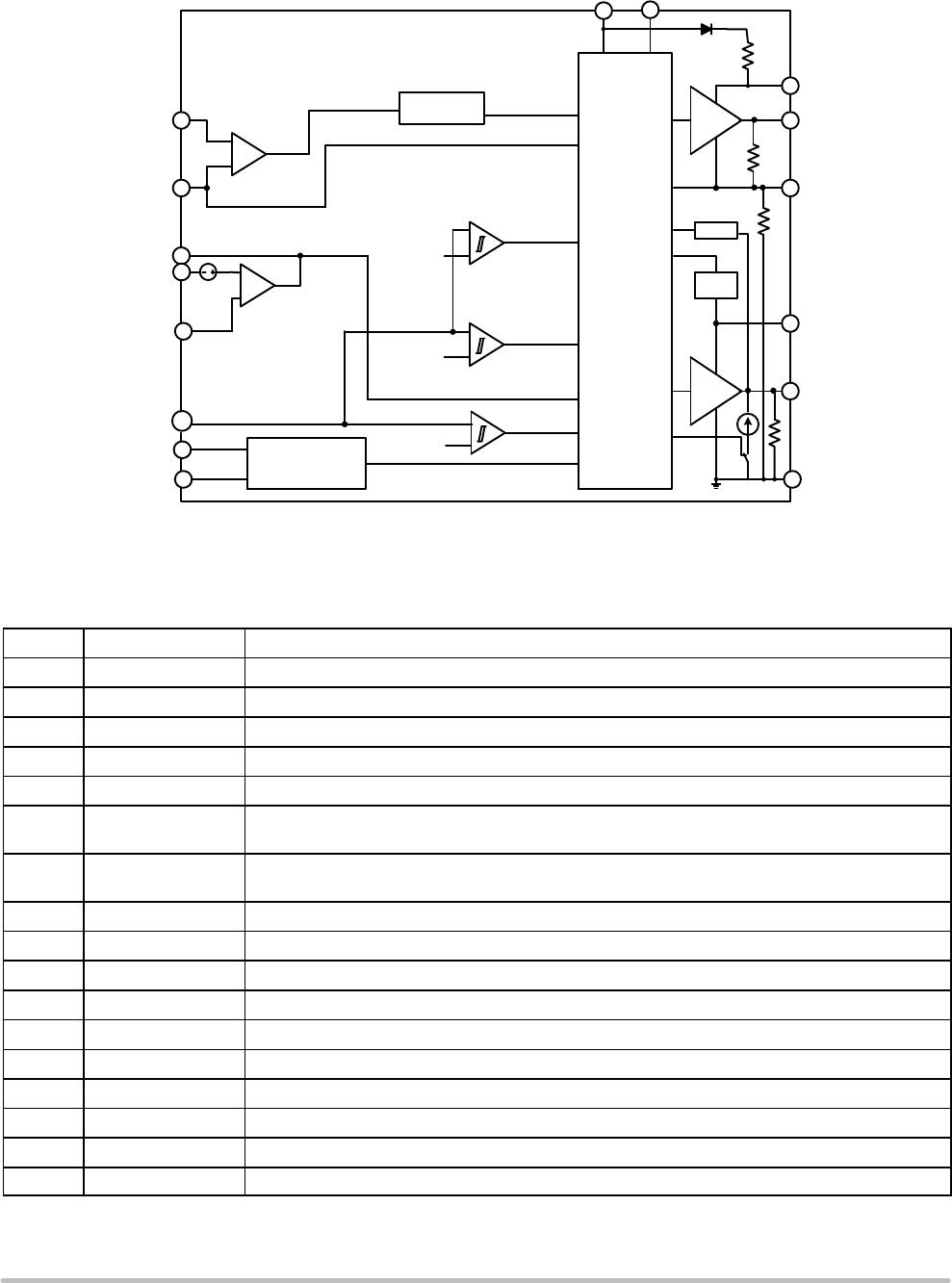
The NCP5230 is a simple single phase solution with differential
phase current sensing, power saving operation, and gate drivers to
provide accurately regulated power.
The adaptive non overlap gate drive and power saving operation
circuit provide a low switching loss and high efficiency solution for
server, notebook, and desktop systems. A high performance
operational error amplifier is provided to simplify compensation of the
system. The NCP5230 features also include soft−start sequence,
accurate overvoltage and over current protection, UVLO for VCC and
VCCP, and thermal shutdown.
Features
• High Performance Operational Error Amplifier
• Internal Soft−Start/Stop
• ±0.5% Internal Voltage Accuracy, 0.8 V voltage reference
• OCP accuracy, Four Re−entry Times Before Latch
• “Lossless” Differential Inductor Current Sensing
• Internal High Precision Current Sensing Amplifier
• Oscillator Frequency Range of 100 kHz − 1000 kHz
• 20 ns Adaptive FET Non−overlap Time of Internal Gate Driver
• 5.0 V to 12 V Operation
• Support 1.5 V to 19 V V
in
• V
out
from 0.8 V to 3.3 V (5 V with 12 V
CC
)
• Chip Enable through OSC pin
• Latched Over Voltage Protection (OVP)
• Internally Fixed OCP Threshold
• Guaranteed Startup Into Pre−Charged Loads
• Thermally Compensated Current Monitoring
• Thermal Shutdown Protection
• Integrated MOSFET Drivers
• Integrated BOOST Diode with internal R
bst
= 2.2 W
• Automatic Power Saving Mode to Maximize Efficiency During Light
Load Operation
• Sync Function
• Remote Ground Sensing
• This is a Pb−Free Device*
Applications
• Desktop and Server Systems
*For additional information on our Pb−Free strategy and soldering details, please
download the ON Semiconductor Soldering and Mounting Techniques
Reference Manual, SOLDERRM/D.
http://onsemi.com
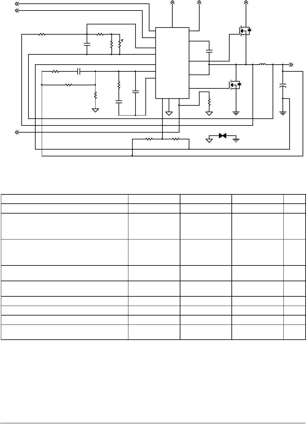
QFN16
CASE 485G
MARKING
DIAGRAMS
4
1
16 13
9
12
58
14
7
15
6
310
211
GNDUG
PGOOD
SYNC
COMP
FB
VSEN
FBG
CSN/VO
BOOT
LX
LG
VCCP
VCC
ROSC/EN
CSP
PIN CONNECTIONS
1
5230
ALYWG
G
5230 = Specific Device Code
A = Assembly Location
L = Wafer Lot
Y = Year
W = Work Week
G = Pb−Free Package
(*Note: Microdot may be in either location)
Device Package Shipping
ORDERING INFORMATION
NCP5230MNTWG QFN16
(Pb−Free)
3000 / Tape & Reel
†For information on tape and reel specifications,
including part orientation and tape sizes, please
refer to our Tape and Reel Packaging Specification
Brochure, BRD8011/D.
(Top View)