NCP5230
http://onsemi.com
5
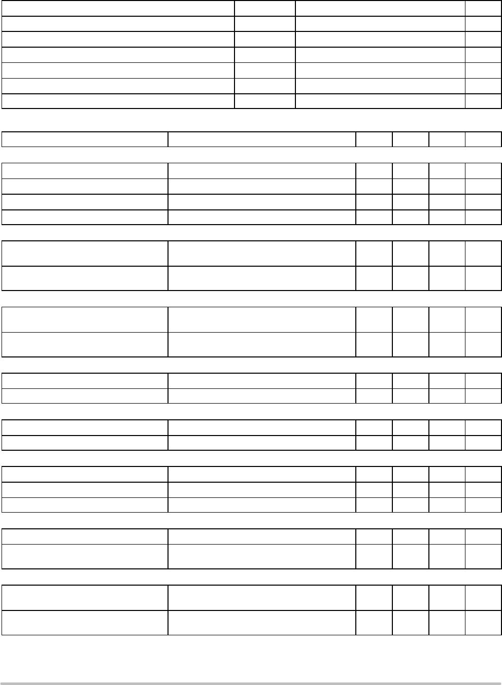
ELECTRICAL CHARACTERISTICS Unless otherwise stated: 0°C < T
A
< 85°C; 4.5 V < VCC < 13.2 V; C
VCC
= 0.1 mF
Parameter UnitMaxTypMinTest Conditions
OSCILLATOR (with no ROSC Resistor Defaults to 200 kHz)
Switching Frequency Accuracy R
OSC
open −10 10 %
OSC Gain (Note 1) 10 kHz /
mA
Disable threshold R
OSC
/EN pin, V
dis_th
0.75 V
MODULATORS (PWM Comparators)
Minimum Pulse Width F
sw
= 200 kHz, OSC open 90 ns
Minimum Turn Off Time (LG on) F
sw
= 200 kHz, OSC open 250 350 450 ns
Magnitude of the PWM Ramp V
IN
= 5 V or 12 V 1.50 V
Maximum Duty Cycle OSC/EN = OPEN 80 95 %
Minimum Skip mode frequency In light load, maximum time for LG to turn on
after HG turns off
30 kHz
SOFT−START
Soft Start Time @ 200 kHz 1024 clock cycles, OSC/EN open 5.12 ms
SOFT−OFF
Soft OFF bleeding resistor R
dis
120
W
OVER CURRENT PROTECTION
First Over Current Threshold CSP−CSN, 4xMasking 17 20 23 mV
Second Over Current Threshold CSP−CSN, Immediate action 30 mV
SYNC PIN
Synchronization Input VIL, square wave 1.0 V
Synchronization Input VIH, square wave 2.5 V
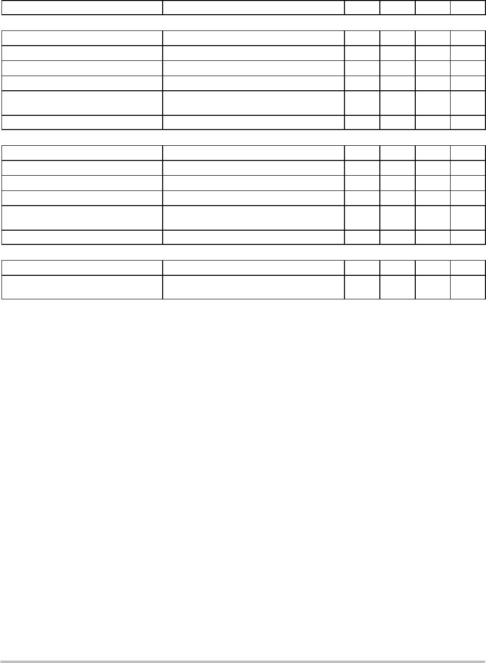
PROTECTION AND PGOOD
Output Voltage Logic Low, Sinking 4 mA 0.4 V
OVP Threshold VSEN rising above 1.25 * V
ref
117 125 130 %
UVP Threshold VSEN falling below 0.75 * V
ref
70 75 80 %
Unlatched Overvoltage Threshold V
th_disoff
with respect to 0.5 V
ref
40 50 60 %
Power Good High Delay (Note 1) 50
ms
Power Good Low Delay (Note 1) 1
ms
ZERO CURRENT DETECTION (LX Pin)
Blanking Time before Zero Current
Detection (Note 1)
Blanking Time after LG is < 1.0 V
40 ns
Capture Time for LX Voltage (Note 1) Time to capture LX voltage once LG is < 1.0 V
(must be within dead time limits)
20 ns
Negative LX detection voltage V
bdls
150 300 450 mV
Positive LX detection voltage V
bdhs
0.2 0.5 1.0 V
Time for V
th
adjustment and settling time
(Note 1)
300 kHz 3.0 3.7
ms
Initial Negative Current Detection
Threshold Voltage Set Point (Note 1)
LX−GND, Includes ± 2 mV Offset Range 1.0 mV
V
th
adjustable Range (Note 1) −16 0 15 mV
1. Guaranteed by design.
2. For propagation delays, ”tpdh” refers to the specified signal going high ”tpdl” refers to it going low. Reference Gate Timing Diagram.