M41ST85W Operating modes
Doc ID 7531 Rev 11 17/43
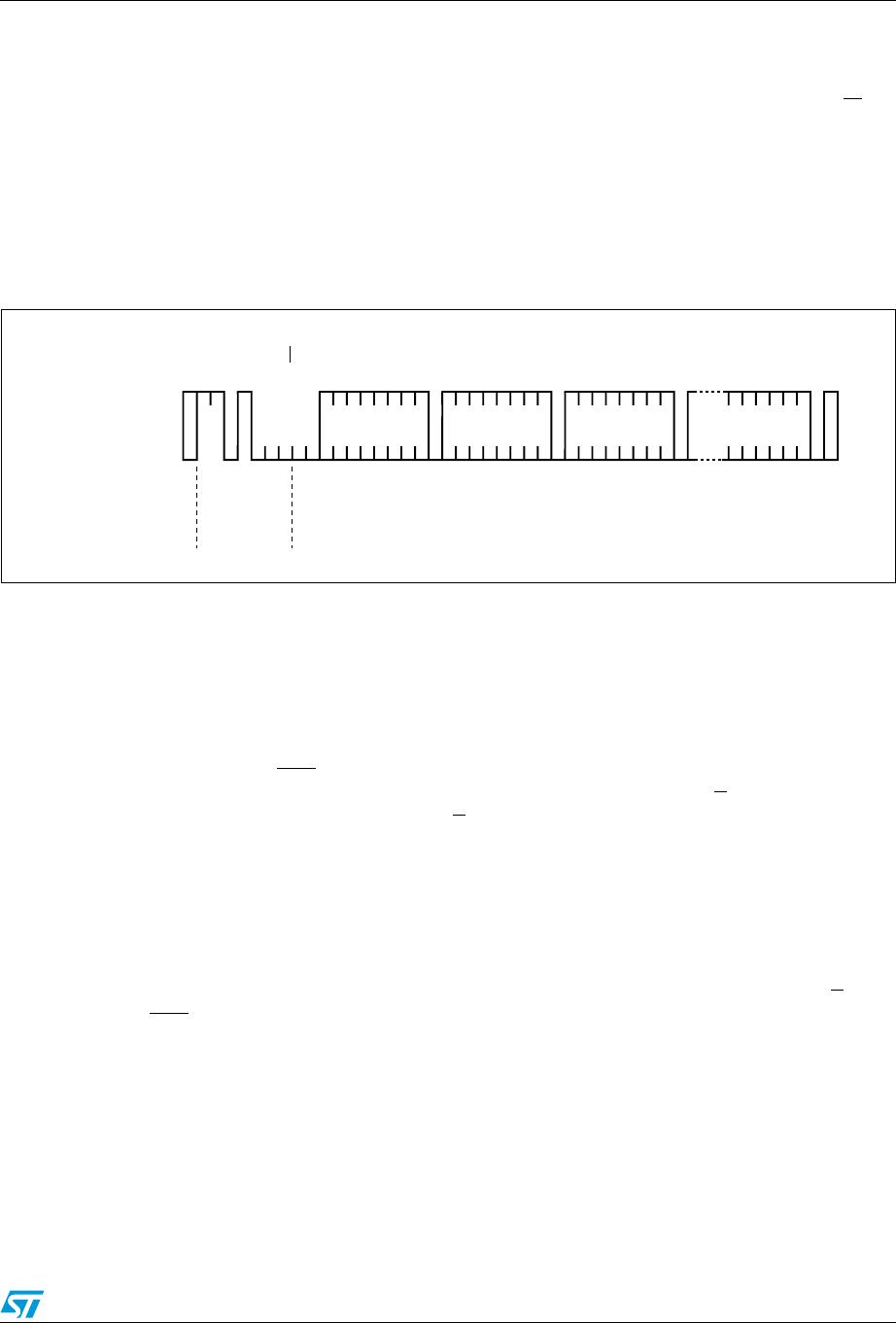
2.3 Write mode
In this mode the master transmitter transmits to the M41ST85W slave receiver. Bus protocol
is shown in Figure 12. Following the START condition and slave address, a logic '0' (R/W
=0)
is placed on the bus and indicates to the addressed device that word address An will follow
and is to be written to the on-chip address pointer. The data word to be written to the
memory is strobed in next and the internal address pointer is incremented to the next
memory location within the RAM on the reception of an acknowledge clock. The M41ST85W
slave receiver will send an acknowledge clock to the master transmitter after it has received
the slave address and again after it has received the word address and each data byte.
Figure 12. Write mode sequence
2.4 Data retention mode
With valid V
CC
applied, the M41ST85W can be accessed as described above with READ or
WRITE cycles. Should the supply voltage decay, the M41ST85W will automatically deselect,
write protecting itself (and any external SRAM) when V
CC
falls between V
PFD
(max) and
V
PFD
(min). This is accomplished by internally inhibiting access to the clock registers. At this
time, the reset pin (RST
) is driven active and will remain active until V
CC
returns to nominal
levels. External RAM access is inhibited in a similar manner by forcing E
CON
to a high level.
This level is within 0.2 volts of the V
BAT
. E
CON
will remain at this level as long as V
CC
remains at an out-of-tolerance condition. When V
CC
falls below the battery backup
switchover voltage (V
SO
), power input is switched from the V
CC
pin to the SNAPHAT
®
battery, and the clock registers and external SRAM are maintained from the attached
battery supply.
All outputs become high impedance. The V
OUT
pin is capable of supplying 100 µA of current
to the attached memory with less than 0.3 volts drop under this condition. On power-up,
when V
CC
returns to a nominal value, write protection continues for t
rec
by inhibiting E
CON
.
The RST
signal also remains active during this time (see Figure 20 on page 33).
Note: Most low power SRAMs on the market today can be used with the M41ST85W RTC
SUPERVISOR. There are, however some criteria which should be used in making the final
choice of an SRAM to use. The SRAM must be designed in a way where the chip enable
input disables all other inputs to the SRAM. This allows inputs to the M41ST85W and
SRAMs to be “Don’t Care” once V
CC
falls below V
PFD
(min). The SRAM should also
guarantee data retention down to V
CC
= 2.0 volts. The chip enable access time must be
sufficient to meet the system needs with the chip enable output propagation delays
included. If the SRAM includes a second chip enable pin (E2), this pin should be tied to
V
OUT
.
AI00591
BUS ACTIVITY:
ACK
S
ACK
ACK
ACK
ACK
STOP
START
PSDA LINE
BUS ACTIVITY:
MASTER
R/W
DATA n DATA n+1 DATA n+X
WORD
ADDRESS (An)
SLAVE
ADDRESS

