M41ST85W Clock operation
Doc ID 7531 Rev 11 19/43
3 Clock operation
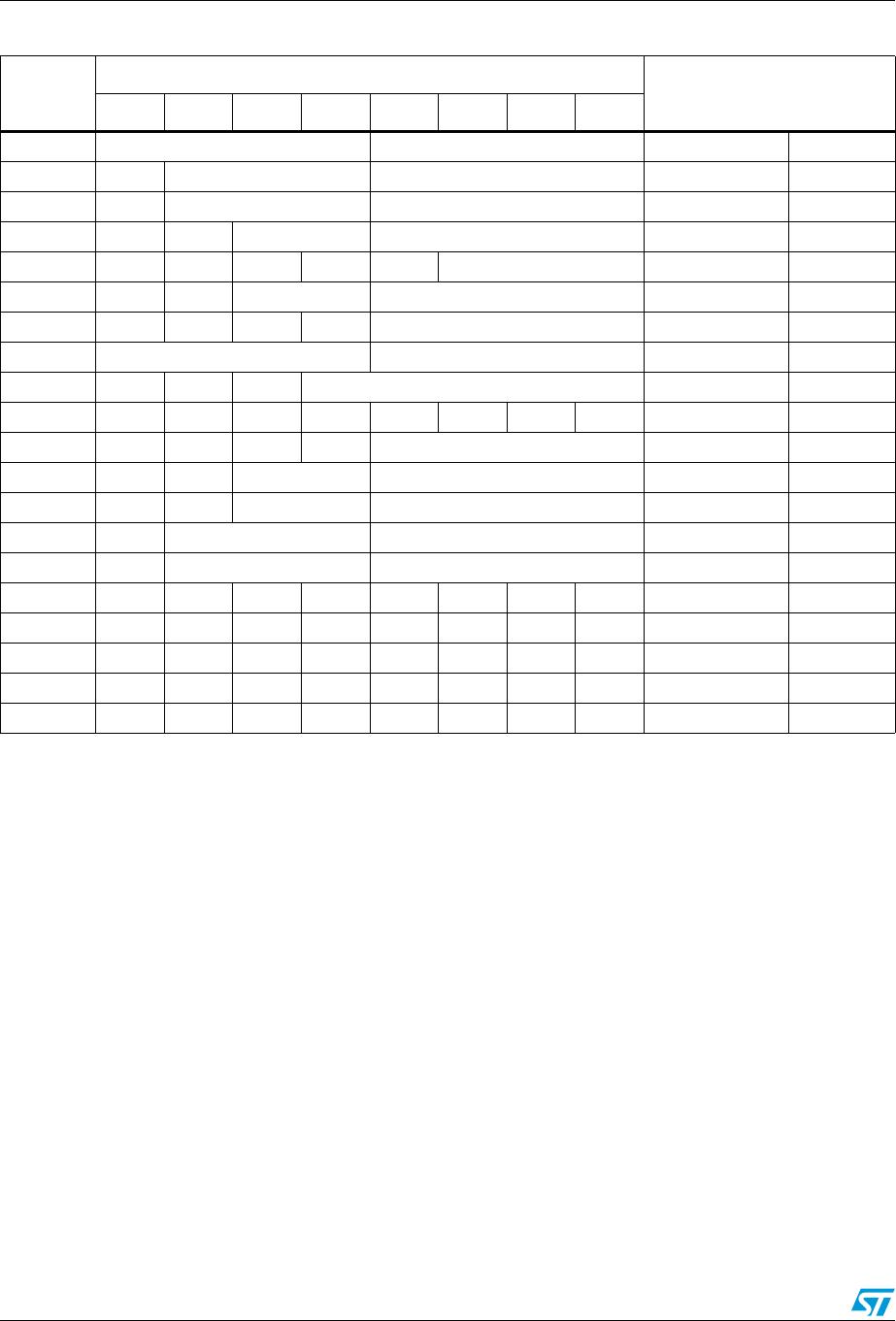
The eight byte clock register (see Table 2 on page 20) is used to both set the clock and to
read the date and time from the clock, in a binary coded decimal format. Tenths/hundredths
of seconds, seconds, minutes, and hours are contained within the first four registers.
Note: A WRITE to any clock register will result in the tenths/hundredths of seconds being reset to
“00,” and tenths/hundredths of seconds cannot be written to any value other than “00.
Bits D6 and D7 of clock register 03h (century/hours register) contain the CENTURY
ENABLE bit (CEB) and the CENTURY bit (CB). Setting CEB to a '1' will cause CB to toggle,
either from '0' to '1' or from '1' to '0' at the turn of the century (depending upon its initial
state). If CEB is set to a '0,' CB will not toggle. Bits D0 through D2 of register 04h contain the
day (day of week). Registers 05h, 06h, and 07h contain the date (day of month), month and
years. The ninth clock register is the control register (this is described in the clock calibration
section). Bit D7 of register 01h contains the STOP bit (ST). Setting this bit to a '1' will cause
the oscillator to stop. If the device is expected to spend a significant amount of time on the
shelf, the oscillator may be stopped to reduce current drain. When reset to a '0' the oscillator
restarts within one second.
The eight clock registers may be read one byte at a time, or in a sequential block. The
control register (address location 08h) may be accessed independently. Provision has been
made to assure that a clock update does not occur while any of the eight clock addresses
are being read. If a clock address is being read, an update of the clock registers will be
halted. This will prevent a transition of data during the READ.
3.1 Power-down time-stamp
When a power failure occurs, the halt update bit (HT) will automatically be set to a '1.' This
will prevent the clock from updating the TIMEKEEPER
®
registers, and will allow the user to
read the exact time of the power-down event. Resetting the HT bit to a '0' will allow the clock
to update the TIMEKEEPER registers with the current time. For more information, see
application note AN1572.
3.2 TIMEKEEPER
®
registers
The M41ST85W offers 20 internal registers which contain clock, alarm, watchdog, flag,
square wave and control data. These registers are memory locations which contain external
(user accessible) and internal copies of the data (usually referred to as BiPORT
TIMEKEEPER cells). The external copies are independent of internal functions except that
they are updated periodically by the simultaneous transfer of the incremented internal copy.
The internal divider (or clock) chain will be reset upon the completion of a WRITE to any
clock address.
The system-to-user transfer of clock data will be halted whenever the address being read is
a clock address (00h to 07h). The update will resume either due to a stop condition or when
the pointer increments to a non-clock or RAM address.
TIMEKEEPER and alarm registers store data in BCD. control, watchdog and square wave
registers store data in binary format.
Clock operation M41ST85W
20/43 Doc ID 7531 Rev 11
Table 2. TIMEKEEPER
®
register map
Address
Data
Function/range
BCD format
D7 D6 D5 D4 D3 D2 D1 D0
00h 0.1 seconds 0.01 seconds Seconds 00-99
01h ST 10 seconds Seconds Seconds 00-59
02h 0 10 minutes Minutes Minutes 00-59
03h CEB CB 10 hours Hours (24-hour format) Century/hours 0-1/00-23
04h TR 0 0 0 0 Day of week Day 01-7
05h 0 0 10 date Date: day of month Date 01-31
06h 0 0 0 10M Month Month 01-12
07h 10 years Year Year 00-99
08h OUT FT S Calibration Control
09h WDS BMB4 BMB3 BMB2 BMB1 BMB0 RB1 RB0 Watchdog
0Ah AFE SQWE ABE Al 10M Alarm month Al month 01-12
0Bh RPT4 RPT5 AI 10 date Alarm date Al date 01-31
0Ch RPT3 HT AI 10 hour Alarm hour Al hour 00-23
0Dh RPT2 Alarm 10 minutes Alarm minutes Al min 00-59
0Eh RPT1 Alarm 10 seconds Alarm seconds Al sec 00-59
0Fh WDF AF 0 BL 0 0 0 0 Flags
10h 0 0 0 0 0 0 0 0 Reserved
11h 0 0 0 0 0 0 0 0 Reserved
12h 0 0 0 0 0 0 0 0 Reserved
13h RS3 RS2 RS1 RS0 0 0 0 0 SQW
Keys: S = Sign bit RB0-RB1 = Watchdog resolution bits
FT = Frequency test bit WDS = Watchdog steering bit
ST = Stop bit ABE = Alarm in battery backup mode enable bit
0 = Must be set to zero RPT1-RPT5 = Alarm repeat mode bits
BL = Battery low flag (read only) WDF = Watchdog flag (read only)
BMB0-BMB4 = Watchdog multiplier bits AF = Alarm flag (read only)
CEB = Century enable bit SQWE = Square wave enable
CB = Century bit RS0-RS3 = SQW frequency
OUT = Output level HT = Halt update bit
AFE = Alarm flag enable flag TR = t
rec
bit
M41ST85W Clock operation
Doc ID 7531 Rev 11 21/43
3.3 Calibrating the clock
The M41ST85W is driven by a quartz controlled oscillator with a nominal frequency of
32,768 Hz. The devices are tested not exceed +/–35 ppm (parts per million) oscillator
frequency error at 25
o
C, which equates to about +/–1.53 minutes per month. When the
Calibration circuit is properly employed, accuracy improves to better than ±2 ppm at 25°C.
The oscillation rate of crystals changes with temperature (see Figure 13 on page 22).
Therefore, the M41ST85W design employs periodic counter correction. The calibration
circuit adds or subtracts counts from the oscillator divider circuit at the divide by 256 stage,
as shown in Figure 14 on page 22. The number of times pulses which are blanked
(subtracted, negative calibration) or split (added, positive calibration) depends upon the
value loaded into the five calibration bits found in the control register. Adding counts speeds
the clock up, subtracting counts slows the clock down.
The calibration bits occupy the five lower order bits (D4-D0) in the control register (08h).
These bits can be set to represent any value between 0 and 31 in binary form. Bit D5 is a
sign bit; '1' indicates positive calibration, '0' indicates negative calibration. Calibration occurs
within a 64 minute cycle. The first 62 minutes in the cycle may, once per minute, have one
second either shortened by 128 or lengthened by 256 oscillator cycles. If a binary '1' is
loaded into the register, only the first 2 minutes in the 64 minute cycle will be modified; if a
binary 6 is loaded, the first 12 will be affected, and so on.
Therefore, each calibration step has the effect of adding 512 or subtracting 256 oscillator
cycles for every 125,829,120 actual oscillator cycles, that is +4.068 or –2.034 ppm of
adjustment per calibration step in the calibration register. Assuming that the oscillator is
running at exactly 32,768 Hz, each of the 31 increments in the calibration byte would
represent +10.7 or –5.35 seconds per month which corresponds to a total range of +5.5 or
–2.75 minutes per month.
Two methods are available for ascertaining how much calibration a given M41ST85W may
require.
The first involves setting the clock, letting it run for a month and comparing it to a known
accurate reference and recording deviation over a fixed period of time. Calibration values,
including the number of seconds lost or gained in a given period, can be found in application
note AN934, “TIMEKEEPER
®
calibration.” This allows the designer to give the end user the
ability to calibrate the clock as the environment requires, even if the final product is
packaged in a non-user serviceable enclosure. The designer could provide a simple utility
that accesses the calibration byte.
The second approach is better suited to a manufacturing environment, and involves the use
of the IRQ
/FT/OUT pin. The pin will toggle at 512 Hz, when the stop bit (ST, D7 of 01h) is '0,'
the frequency test bit (FT, D6 of 08h) is '1,' the alarm flag enable bit (AFE, D7 of 0Ah) is '0,'
and the watchdog steering bit (WDS, D7 of 09h) is '1' or the watchdog register (09h = 0) is
reset.
Any deviation from 512 Hz indicates the degree and direction of oscillator frequency shift at
the test temperature. For example, a reading of 512.010124 Hz would indicate a +20 ppm
oscillator frequency error, requiring a –10 (XX001010) to be loaded into the calibration byte
for correction. Note that setting or changing the calibration byte does not affect the
frequency test output frequency.
The IRQ
/FT/OUT pin is an open drain output which requires a pull-up resistor to V
CC
for
proper operation. A 500 to 10 k resistor is recommended in order to control the rise time.
The FT bit is cleared on power-down.

M41ST85WMH6F

Mfr. #:
Manufacturer:
STMicroelectronics
Description:
Real Time Clock Serial 512 (64x8)
Lifecycle:
New from this manufacturer.
Delivery:
DHL FedEx Ups TNT EMS
Payment:
T/T Paypal Visa MoneyGram Western Union

Products related to this Datasheet