5
FN8177.7
October 7, 2015
Submit Document Feedback
Absolute Maximum Ratings Recommended Operating Conditions
Temperature Under Bias . . . . . . . . . . . . . . . . . . . . .-65°C to +135°C
Storage Temperature . . . . . . . . . . . . . . . . . . . . . . . .-65°C to +150°C
Voltage on CS
, INC, U/D, and
V
CC
with Respect to V
SS
. . . . . . . . . . . . . . . . . . . . . . . -1V to +7V
Voltage on V
H
, V
L
, V
W
with respect to V
SS
. . . . . . . . . . . . . . . . . . . . . . . . . . . . -6V to +7V
V = |V
H
- V
L
|:
X9313Z . . . . . . . . . . . . . . . . . . . . . . . . . . . . . . . . . . . . . . . . . . . .4V
X9313W, X9313U . . . . . . . . . . . . . . . . . . . . . . . . . . . . . . . . . . .10V
I
W
(10s) . . . . . . . . . . . . . . . . . . . . . . . . . . . . . . . . . . . . . . . . .±8.8mA
ESD Rating
Human Body Model . . . . . . . . . . . . . . . . . . . . . . . . . . . . . . . 2.0kV
Machine Model . . . . . . . . . . . . . . . . . . . . . . . . . . . . . . . . . . . .200V
Temperature:
Commercial. . . . . . . . . . . . . . . . . . . . . . . . . . . . . . . . 0°C to +70°C
Industrial . . . . . . . . . . . . . . . . . . . . . . . . . . . . . . . . .-40°C to +85°C
Supply Voltage (VCC):
X9313 . . . . . . . . . . . . . . . . . . . . . . . . . . . . . . . . . . . . . . . .5V ±10%
X9313-3 . . . . . . . . . . . . . . . . . . . . . . . . . . . . . . . . . . . . 3V to 5.5V
Max Wiper current . . . . . . . . . . . . . . . . . . . . . . . . . . . . . . . . .±4.4mA
Power rating:
R
TOTAL
10k . . . . . . . . . . . . . . . . . . . . . . . . . . . . . . . . . .10mW
R
TOTAL
1k . . . . . . . . . . . . . . . . . . . . . . . . . . . . . . . . . . . . .16mW
Pb-free reflow profile . . . . . . . . . . . . . . . . . . . . . . . . . .see link below
http://www.intersil.com/pbfree/Pb-FreeReflow.asp
Pb-free PDIPs can be used for through hole wave solder processing
only. They are not intended for use in Reflow solder processing
applications
CAUTION: Do not operate at or near the maximum ratings listed for extended periods of time. Exposure to such conditions may adversely impact product reliability and
result in failures not covered by warranty.
Potentiometer Characteristics Over recommended operating conditions, unless otherwise stated.
SYMBOL PARAMETER TEST CONDITIONS
LIMITS
UNITMIN TYP MAX
End-to-end Resistance Tolerance ±20 %
V
VH
V
H
Terminal Voltage -V
CC
+V
CC
V
V
VL
V
L
Terminal Voltage -V
CC
+V
CC
V
R
W
Wiper Resistance I
W
= (V
H
- V
L
)/R
TOTAL
, V
CC
= 5V 40 100
I
W
Wiper Current ±4.4 mA
Noise (Note 5) Ref: 1kHz -120 dBV
Resolution 3%
Absolute Linearity (Note 1) R
W(n)(actual)
- R
W(n)(expected)
±1 MI
(Note 3)
Relative Linearity (Note 2) R
W(n+1)
- (R
W(n)
+MI) ±0.2 MI
(Note 3)
R
TOTAL
Temperature Coefficient (Note 5) ±300 ppm/°C
Ratiometric Temperature Coefficient
(Note 5)
±20 ppm/°C
C
H
/C
L
/C
W
(Note 5)
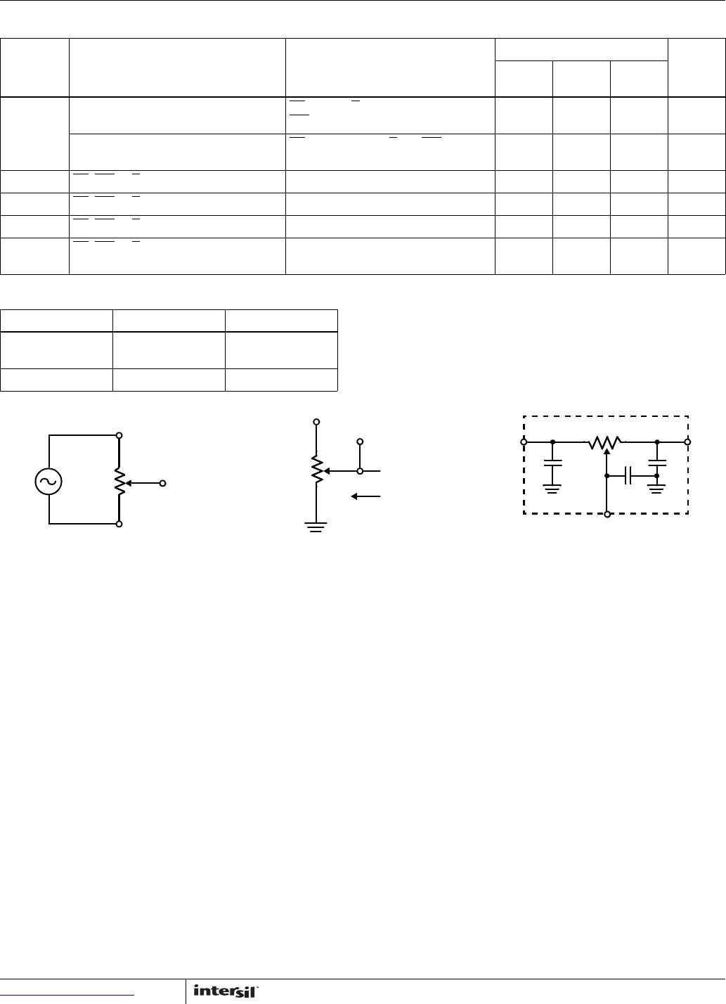
Potentiometer Capacitances See Circuit #3 10/10/25 pF
NOTES:
1. Absolute linearity is utilized to determine actual wiper voltage versus expected voltage = (V
W(n)(actual)
- V
W(n)(expected)
) = ±1 MI maximum.
2. Relative linearity is a measure of the error in step size between taps = R
W(n+1)
- (R
W(n)
+ MI) = ±0.2 MI.
3. 1 MI = minimum increment = R
TOT
/31.
X9313