7
FN8177.7
October 7, 2015
Submit Document Feedback
Power-Up and Power-Down Requirements
The recommended power-up sequence is to apply V
CC
/V
SS
first, then the potentiometer voltages. During power-up, the
data sheet parameters for the DCP do not fully apply until
1ms after V
CC
reaches its final value. The V
CC
ramp
specification is always in effect. In order to prevent unwanted
tap position changes, or an inadvertent store, bring the CS
and INC
high before or concurrently with the VCC pin on
power-up.
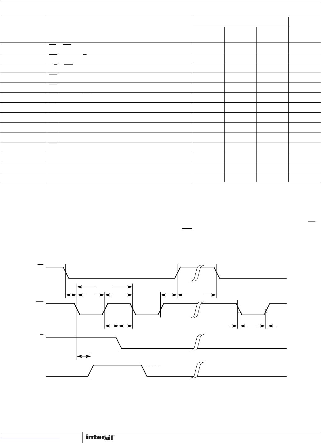
AC Electrical Specifications Over recommended operating conditions, unless otherwise stated.
SYMBOL PARAMETER
LIMITS
UNITMIN
TYP
(Note 4) MAX
t
CI
CS to INC Setup 100 ns
t
ID
INC HIGH to U/D Change 100 ns
t
DI
U/D to INC Setup 2.9 µs
t
IL
INC LOW Period 1 µs
t
IH
INC HIGH Period 1 µs
t
IC
INC Inactive to CS Inactive 1 µs
t
CPH
CS Deselect Time (STORE) 20 ms
t
CPH
CS Deselect Time (NO STORE) 100 ns
t
IW
INC to V
W
Change 5 µs
t
CYC
INC Cycle Time 2 µs
t
R
, t
F
(Note 5) INC Input Rise and Fall Time 500 µs
t
PU
(Note 5) Power-up to Wiper Stable 10 µs
t
R
V
CC
(Note 5) V
CC
Power-up Rate 0.2 50 V/ms
t
WR
(Note 5) Store Cycle 10 ms
NOTES:
4. Typical values are for T
A
= +25°C and nominal supply voltage.
5. This parameter is not 100% tested.
CS
INC
U/D
V
W
t
CI
t
IL
t
IH
t
CYC
t
ID
t
DI
t
IW
MI
(SEE NOTE)
t
IC
t
CPH
t
F
t
R
10%
90% 90%
NOTE: MI IN THE AC TIMING DIAGRAM REFERS TO THE MINIMUM INCREMENTAL CHANGE IN THE V
W
OUTPUT DUE TO A CHANGE IN
THE WIPER POSITION.
FIGURE 4. AC TIMING DIAGRAM
X9313
8
FN8177.7
October 7, 2015
Submit Document Feedback
Applications Information
Electronic digitally controlled potentiometers (XDCP) provide
three powerful application advantages:
1. The variability and reliability of a solid-state potentiometer.
2. The flexibility of computer-based digital controls.
3. The retentivity of nonvolatile memory used for the storage
of multiple potentiometer settings or data.
Basic Configurations of Electronic Potentiometers
Basic Circuits
V
R
V
W
/R
W
V
R
I
THREE-TERMINAL POTENTIOMETER;
VARIABLE VOLTAGE DIVIDER
TWO-TERMINAL VARIABLE RESISTOR;
VARIABLE CURRENT
V
H
V
L
CASCADING TECHNIQUESBUFFERED REFERENCE VOLTAGE
+
+5V
R
1
+V
-5V
VW
V
REF
V
OUT
OP-07
V
W
VW/RW
+V
+V +V
X
(a) (b)
V
OUT
= V
W
/R
W
NONINVERTING AMPLIFIER
+
V
S
V
O
R
2
R
1
V
O
= (1 + R
2
/R
1
)V
S
LM308A
VOLTAGE REGULATOR
R
1
R
2
I
adj
V
O
(REG) = 1.25V (1 + R
2
/R
1
) + I
ADJ
R
2
V
O
(REG)V
IN
317
OFFSET VOLTAGE ADJUSTMENT
+
V
S
V
O
R
2
R
1
100k
10k10k
10k
-12V+12V
TL072
COMPARATOR WITH HYSTERESIS
V
UL
= [R
1
/(R
1
+ R
2
)] V
O
(max)
V
LL
= [R
1
/(R
1
+ R
2
)] V
O
(min)
+
V
S
V
O
R
2
R
1
}
}
LT311A
+5V
-5V
(FOR ADDITIONAL CIRCUITS SEE AN115)
X9313
9
FN8177.7
October 7, 2015
Submit Document Feedback
About Intersil
Intersil Corporation is a leading provider of innovative power management and precision analog solutions. The company's products
address some of the largest markets within the industrial and infrastructure, mobile computing and high-end consumer markets.
For the most updated datasheet, application notes, related documentation and related parts, please see the respective product
information page found at www.intersil.com.
You may report errors or suggestions for improving this datasheet by visiting www.intersil.com/ask.
Reliability reports are also available from our website at www.intersil.com/support
Revision History
The revision history provided is for informational purposes only and is believed to be accurate, but not warranted. Please go to the web to make
sure that you have the latest revision.
DATE REVISION CHANGE
October 7, 2015 FN8177.7 Added Revision History beginning with Rev 7.
Added About Intersil Verbiage.
Updated Ordering Information on page 2.
DC Electrical Spec Table on page 6 - changed I
CC
for Parameter V
CC
Active Current to I
SB
Updated POD M8.118 to most current revision with changes as follows:
Corrected lead width dimension in side view 1 from "0.25 - 0.036" to "0.25 - 0.36"
Updated to new intersil format by adding land pattern and moving dimensions
from table onto drawing.
Updated POD M8.15 to most current revision with changes as follows:
Changed Note 1 "1982" to "1994"
Changed in Typical Recommended Land Pattern the following:
2.41(0.095) to 2.20(0.087)
0.76 (0.030) to 0.60(0.023)
0.200 to 5.20(0.205)
Updated to new POD format by removing table and moving dimensions onto
drawing and adding land pattern.
X9313
X9313ZMZT1

Mfr. #:
Manufacturer:
Renesas / Intersil
Description:
Digital Potentiometer ICs CMOS EEPOT 1KOHM 32 TAPS
Lifecycle:
New from this manufacturer.
Delivery:
DHL FedEx Ups TNT EMS
Payment:
T/T Paypal Visa MoneyGram Western Union