5
IDT72V201/72V211/72V221/72V231/72V241/72V251 3.3V CMOS SyncFIFO™
256 x 9, 512 x 9, 1,024 x 9, 2,048 x 9, 4,096 x 9 and 8,192 x 9
COMMERCIAL AND INDUSTRIAL
TEMPERATURE RANGES
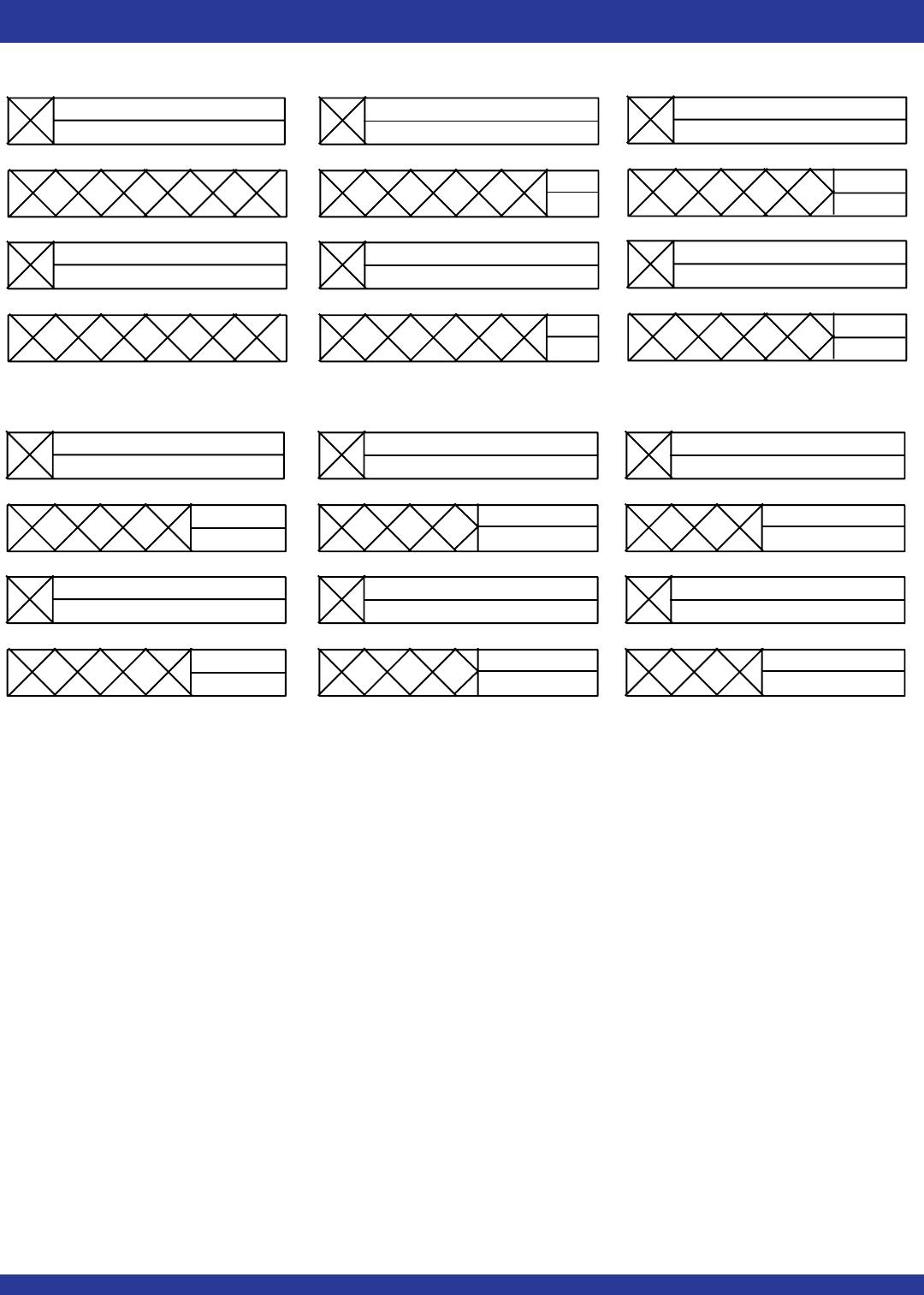
LD WEN1 WCLK Selection
0 0 Empty Offset (LSB)
Empty Offset (MSB)
Full Offset (LSB)
Full Offset (MSB)
0 1 No Operation
1 0 Write Into FIFO
1 1 No Operation
Figure 2. Write Offset Register
NOTES:
1. For the purposes of this table, WEN2 = VIH.
2. The same selection sequence applies to reading from the registers. REN1 and REN2
are enabled and read is performed on the LOW-to-HIGH transition of RCLK.
SIGNAL DESCRIPTIONS
INPUTS:
DATA IN (D0 - D8)
Data inputs for 9-bit wide data.
CONTROLS:
RESET (RS)
Reset is accomplished whenever the Reset (RS) input is taken to a LOW state.
During reset, both internal read and write pointers are set to the first location.
A reset is required after power-up before a write operation can take place. The
Full Flag (FF) and Programmable Almost-Full Flag (PAF) will be reset to HIGH
after t
RSF
. The Empty Flag (EF) and Programmable Almost-Empty Flag (PAE)
will be reset to LOW after t
RSF
. During reset, the output register is initialized to
all zeros and the offset registers are initialized to their default values.
WRITE CLOCK (WCLK)
A write cycle is initiated on the LOW-to-HIGH transition of the Write Clock
(WCLK). Data setup and hold times must be met in respect to the LOW-to-HIGH
transition of the Write Clock (WCLK). The Full Flag (FF) and Programmable
Almost-Full Flag (PAF) are synchronized with respect to the LOW-to-HIGH
transition of the Write Clock (WCLK).
The Write and Read clocks can be asynchronous or coincident.
WRITE ENABLE 1 (WEN1)
If the FIFO is configured for programmable flags, Write Enable 1 (WEN1)
is the only enable control pin. In this configuration, when Write Enable 1 (WEN1)
is low, data can be loaded into the input register and RAM array on the LOW-
to-HIGH transition of every Write Clock (WCLK). Data is stored in the RAM array
sequentially and independently of any on-going read operation.
In this configuration, when Write Enable 1 (WEN1) is HIGH, the input register
holds the previous data and no new data is allowed to be loaded into the register.
If the FIFO is configured to have two write enables, which allows for depth
expansion, there are two enable control pins. See Write Enable 2 paragraph
below for operation in this configuration.
To prevent data overflow, the Full Flag (FF) will go LOW, inhibiting further
write operations. Upon the completion of a valid read cycle, the Full Flag (FF)
will go HIGH after tWFF, allowing a valid write to begin. Write Enable 1 (WEN1)
is ignored when the FIFO is full.
READ CLOCK (RCLK)
Data can be read on the outputs on the LOW-to-HIGH transition of the Read
Clock (RCLK). The Empty Flag (EF) and Programmable Almost-Empty Flag
(PAE) are synchronized with respect to the LOW-to-HIGH transition of the Read
Clock (RCLK).
The Write and Read clocks can be asynchronous or coincident.
READ ENABLES (REN1, REN2)
When both Read Enables (REN1, REN2) are LOW, data is read from the
RAM array to the output register on the LOW-to-HIGH transition of the Read
Clock (RCLK).
When either Read Enable (REN1, REN2) is HIGH, the output register holds
the previous data and no new data is allowed to be loaded into the register.
When all the data has been read from the FIFO, the Empty Flag (EF) will go
LOW, inhibiting further read operations. Once a valid write operation has been
accomplished, the Empty Flag (EF) will go HIGH after t
REF
and a valid read can
begin. The Read Enables (REN1, REN2) are ignored when the FIFO is empty.
OUTPUT ENABLE (OE)
When Output Enable (OE) is enabled (LOW), the parallel output buffers
receive data from the output register. When Output Enable (OE) is disabled
(HIGH), the Q output data bus is in a high-impedance state.
WRITE ENABLE 2/LOAD (WEN2/LD)
This is a dual-purpose pin. The FIFO is configured at Reset to have
programmable flags or to have two write enables, which allows depth expansion.
If Write Enable 2/Load (WEN2/LD) is set high at Reset (RS = LOW), this pin
operates as a second Write Enable pin.
If the FIFO is configured to have two write enables, when Write Enable
(WEN1) is LOW and Write Enable 2/Load (WEN2/LD) is HIGH, data can be
loaded into the input register and RAM array on the LOW-to-HIGH transition
of every Write Clock (WCLK). Data is stored in the RAM array sequentially and
independently of any on-going read operation.
In this configuration, when Write Enable (WEN1) is HIGH and/or Write
Enable 2/Load (WEN2/LD) is LOW, the input register holds the previous data
and no new data is allowed to be loaded into the register.
To prevent data overflow, the Full Flag (FF) will go LOW, inhibiting further
write operations. Upon the completion of a valid read cycle, the Full Flag (FF)
will go HIGH after t
WFF, allowing a valid write to begin. Write Enable 1 (WEN1)
and Write Enable 2/Load (WEN2/LD) are ignored when the FIFO is full.
The FIFO is configured to have programmable flags when the Write Enable
2/Load (WEN2/LD) is set LOW at Reset (RS = LOW). The IDT72V201/72V211/
72V221/72V231/72V241/72V251 devices contain four 8-bit offset registers
which can be loaded with data on the inputs, or read on the outputs. See Figure
3 for details of the size of the registers and the default values.
If the FIFO is configured to have programmable flags when the Write Enable
1 (WEN1) and Write Enable 2/Load (WEN2/LD) are set low, data on the inputs
D is written into the Empty (Least Significant Bit) Offset register on the first LOW-
to-HIGH transition of the Write Clock (WCLK). Data is written into the Empty (Most
Significant Bit) Offset register on the second LOW-to-HIGH transition of the Write
Clock (WCLK), into the Full (Least Significant Bit) Offset register on the third
transition, and into the Full (Most Significant Bit) Offset register on the fourth
transition. The fifth transition of the Write Clock (WCLK) again writes to the Empty
(Least Significant Bit) Offset register.
However, writing all offset registers does not have to occur at one time. One
or two offset registers can be written and then by bringing the Write Enable 2/
Load (WEN2/LD) pin HIGH, the FIFO is returned to normal read/write
operation. When the Write Enable 2/Load (WEN2/LD) pin is set LOW, and Write
Enable 1 (WEN1) is LOW, the next offset register in sequence is written.
The contents of the offset registers can be read on the output lines when the
Write Enable 2/Load (WEN2/LD) pin is set low and both Read Enables (REN1,
REN2) are set LOW. Data can be read on the LOW-to-HIGH transition of the
Read Clock (RCLK).
A read and write should not be performed simultaneously to the offset
registers.