7
IDT72V201/72V211/72V221/72V231/72V241/72V251 3.3V CMOS SyncFIFO™
256 x 9, 512 x 9, 1,024 x 9, 2,048 x 9, 4,096 x 9 and 8,192 x 9
COMMERCIAL AND INDUSTRIAL
TEMPERATURE RANGES
OUTPUTS:
FULL FLAG (FF)
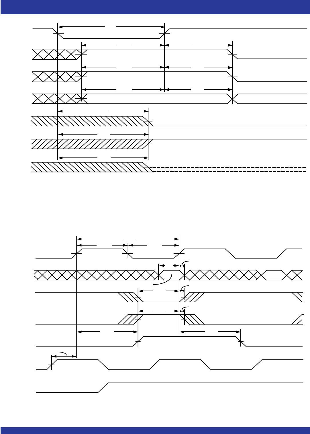
The Full Flag (FF) will go LOW, inhibiting further write operation, when the
device is full. If no reads are performed after Reset (RS), the Full Flag (FF)
will go LOW after 256 writes for the IDT72V201, 512 writes for the IDT72V211,
1,024 writes for the IDT72V221, 2,048 writes for the IDT72V231, 4,096 writes
for the IDT72V241 and 8,192 writes for the IDT72V251.
The Full Flag (FF) is synchronized with respect to the LOW-to-HIGH
transition of the Write Clock (WCLK).
EMPTY FLAG (EF)
The Empty Flag (EF) will go LOW, inhibiting further read operations, when
the read pointer is equal to the write pointer, indicating the device is empty.
The Empty Flag (EF) is synchronized with respect to the LOW-to-HIGH
transition of the Read Clock (RCLK).
PROGRAMMABLE ALMOST-FULL FLAG (PAF)
The Programmable Almost-Full flag (PAF) will go LOW when the FIFO
reaches the almost-full condition. If no reads are performed after Reset (RS),
the Programmable Almost-Full flag (PAF) will go LOW after (256-m) writes for
the IDT72V201, (512-m) writes for the IDT72V211, (1,024-m) writes for the
IDT72V221, (2,048-m) writes for the IDT72V231, (4,096-m) writes for the
IDT72V241 and (8,192-m) writes for the IDT72V251. The offset “m” is defined
in the Full Offset registers.
If there is no full offset specified, the Programmable Almost-Full flag (PAF)
will go LOW at Full-7 words.
The Programmable Almost-Full flag (PAF) is synchronized with respect to
the LOW-to-HIGH transition of the Write Clock (WCLK).
PROGRAMMABLE ALMOST-EMPTY FLAG (PAE)
The Programmable Almost-Empty flag (PAE) will go LOW when the read
pointer is "n+1" locations less than the write pointer. The offset "n" is defined
in the Empty Offset registers. If no reads are performed after Reset the
Programmable Almost-Empty flag (PAE) will go HIGH after "n+1" for the
IDT72V201/72V211/72V221/72V231/72V241/72V251.
If there is no empty offset specified, the Programmable Almost-Empty flag
(PAE) will go LOW at Empty+7 words.
The Programmable Almost-Empty flag (PAE) is synchronized with respect
to the LOW-to-HIGH transition of the Read Clock (RCLK).
DATA OUTPUTS (Q0 - Q8)
Data outputs for a 9-bit wide data.
NUMBER OF WORDS IN FIFO
IDT72V201 IDT72V211 IDT72V221 FF PAF PA E EF
00 0HHLL
1 to n
(1)
1 to n
(1)
1 to n
(1)
HH LH
(n+1) to (256-(m+1)) (n+1) to (512-(m+1)) (n+1) to (1,024-(m+1)) HHHH
(256-m)
(2)
to 255 (512-m)
(2)
to 511 (1,024-m)
(2)
to 1,023 H L H H
256 512 1,024 L L H H
NUMBER OF WORDS IN FIFO
IDT72V231 IDT72V241 IDT72V251 FF PAF PA E EF
000HHLL
1 to n
(1)
1 to n
(1)
1 to n
(1)
HH LH
(n+1) to (2,048-(m+1)) (n+1) to (4,096-(m+1)) (n+1) to (8,192-(m+1)) HHHH
(2,048-m)
(2)
to 2,047 (4,096-m)
(2)
to 4,095 (8,192-m)
(2)
to 8,191 H L H H
2,048 4,096 8,192 L L H H
NOTES:
1. n = Empty Offset (n = 7 default value)
2. m = Full Offset (m = 7 default value)
TABLE 1 — STATUS FLAGS