© Semiconductor Components Industries, LLC, 2011
June, 2011 − Rev. 2
1 Publication Order Number:
MC74HCT4051A/D
MC74HCT4051A,
MC74HCT4052A,
MC74HCT4053A
Analog Multiplexers /
Demultiplexers with LSTTL
Compatible Inputs
High−Performance Silicon−Gate CMOS
The MC74HCT4051A, MC74HCT4052A and MC74HCT4053A
utilize silicon−gate CMOS technology to achieve fast propagation
delays, low ON resistances, and low OFF leakage currents. These
analog multiplexers/demultiplexers control analog voltages that may
vary across the complete power supply range (from V
CC
to V
EE
).
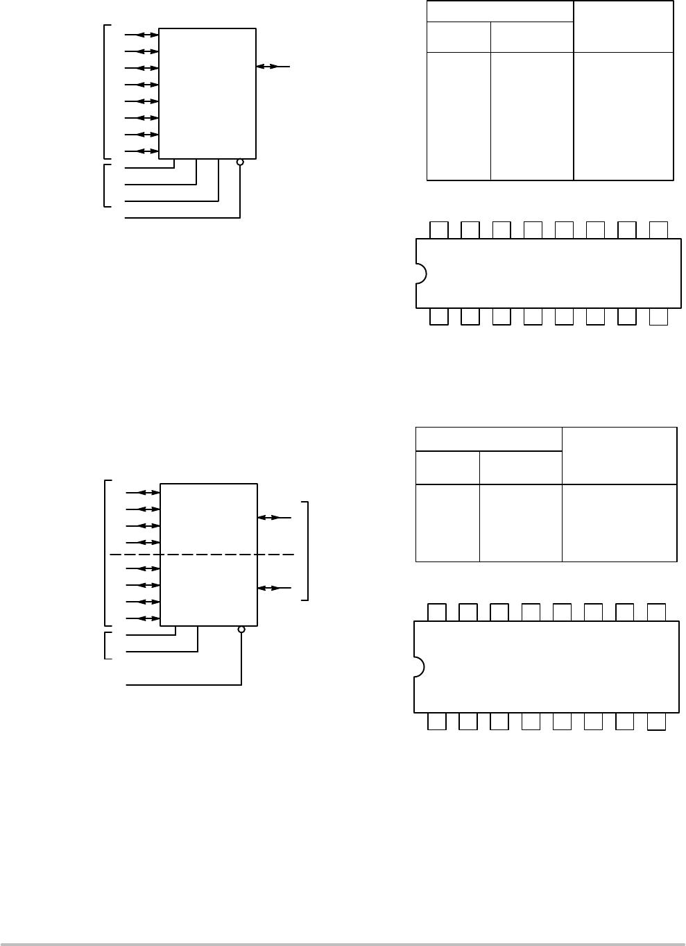
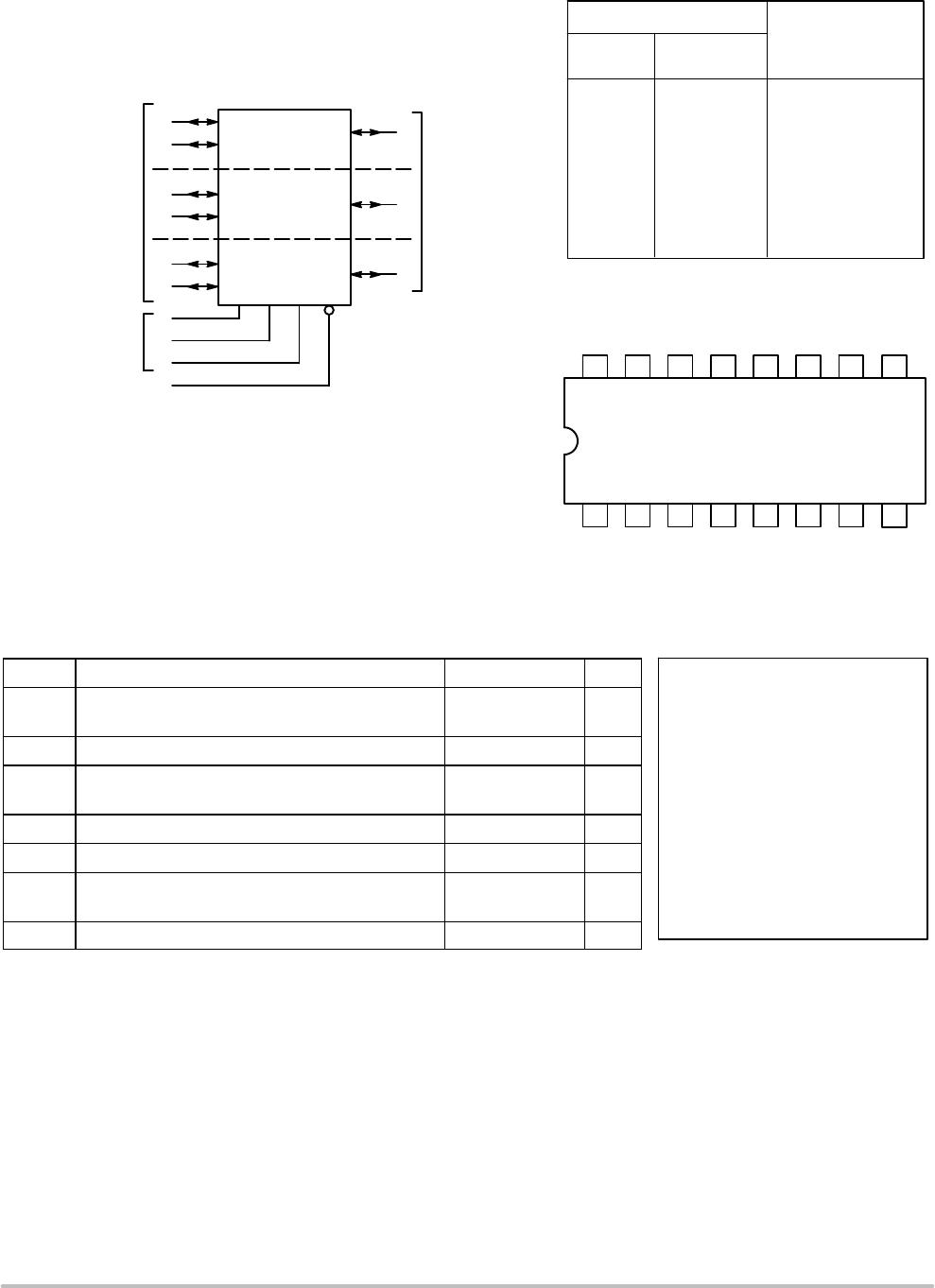
The HCT4051A, HCT4052A and HCT4053A are identical in
pinout to the metal−gate MC14051AB, MC14052AB and
MC14053AB. The Channel−Select inputs determine which one of the
Analog Inputs/Outputs is to be connected, by means of an analog
switch, to the Common Output/Input. When the Enable pin is HIGH,
all analog switches are turned off.
The Channel−Select and Enable inputs are compatible with standard
CMOS and LSTTL outputs.
These devices have been designed so that the ON resistance (R
on
) is
more linear over input voltage than R
on
of metal−gate CMOS analog
switches.
For a multiplexer/demultiplexer with injection current protection,
see HC4851A and HCT4851A.
Features
• Fast Switching and Propagation Speeds
• Low Crosstalk Between Switches
• Diode Protection on All Inputs/Outputs
• Analog Power Supply Range (V
CC
− V
EE
) = 2.0 to 12.0 V
• Digital (Control) Power Supply Range (V
CC
− GND) = 2.0 to 6.0 V
• Improved Linearity and Lower ON Resistance Than Metal−Gate
Counterparts
• Low Noise
• In Compliance with the Requirements of JEDEC Standard No. 7 A
• Chip Complexity: HCT4051A − 184 FETs or 46 Equivalent Gates
HCT4052A − 168 FETs or 42 Equivalent Gates
HCT4053A − 156 FETs or 39 Equivalent Gates
• These Devices are Pb−Free and are RoHS Compliant
http://onsemi.com
MARKING
DIAGRAMS
SOIC−16
D SUFFIX
CASE 751B
TSSOP−16
DT SUFFIX
CASE 948F
1
16
1
16
1
16
HCT405xAG
AWLYWW
HCT40
5xA
ALYWG
G
1
16
SOIC−16 WIDE
DW SUFFIX
CASE 751G
1
16
HCT405xA
AWLYWWG
See detailed ordering and shipping information in the package
dimensions section on page 13 of this data sheet.
ORDERING INFORMATION
1
16
x = 1, 2, 3
A = Assembly Location
WL, L = Wafer Lot
YY, Y = Year
WW, W = Work Week
G or G = Pb−Free Package
(Note: Microdot may be in either location)