MC74HCT4051A, MC74HCT4052A, MC74HCT4053A
http://onsemi.com
10
R
L
Figure 18. Crosstalk Between Any Two
Switches, Test Set−Up
Figure 19. Power Dissipation Capacitance,
Test Set−Up
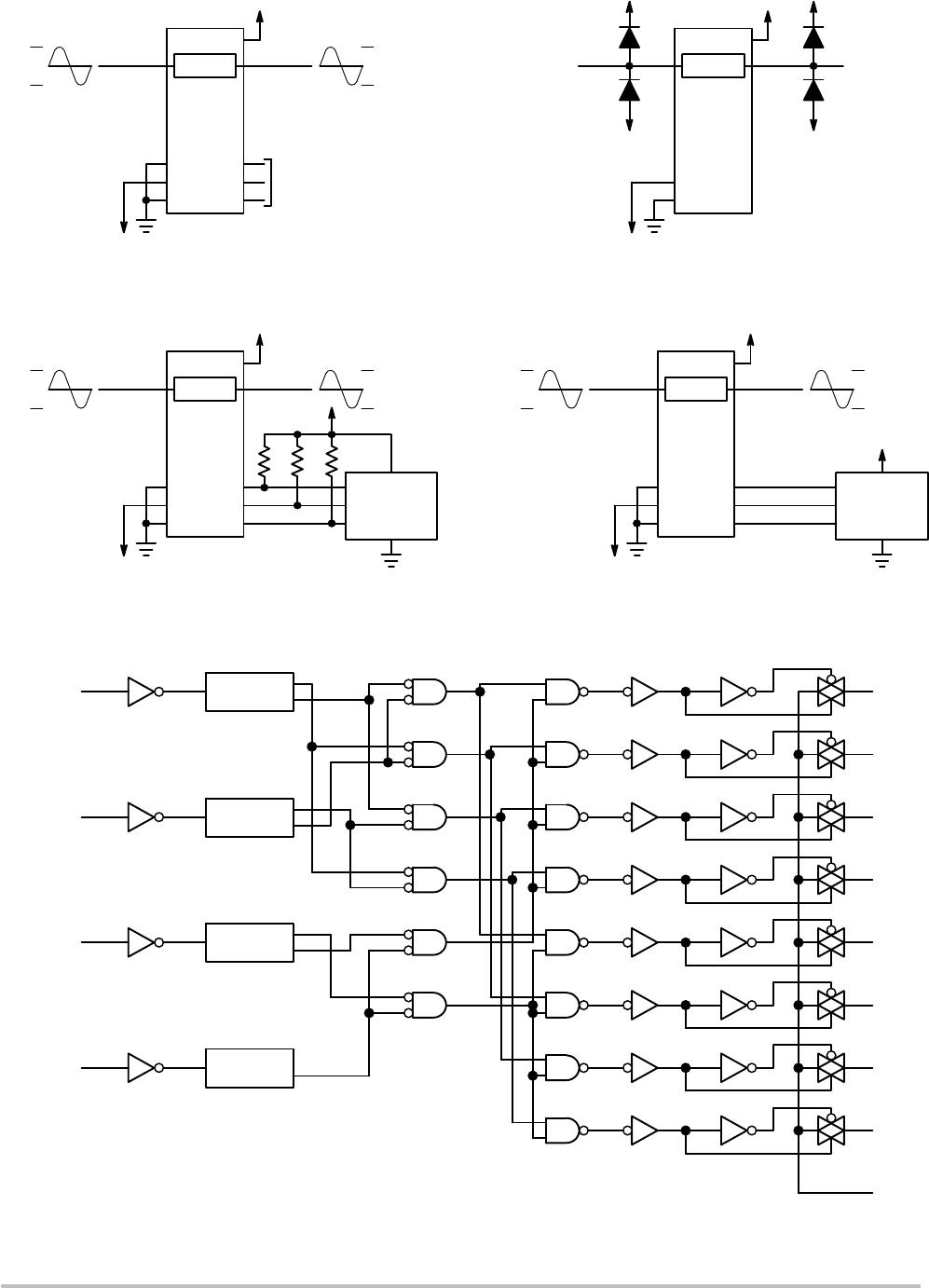
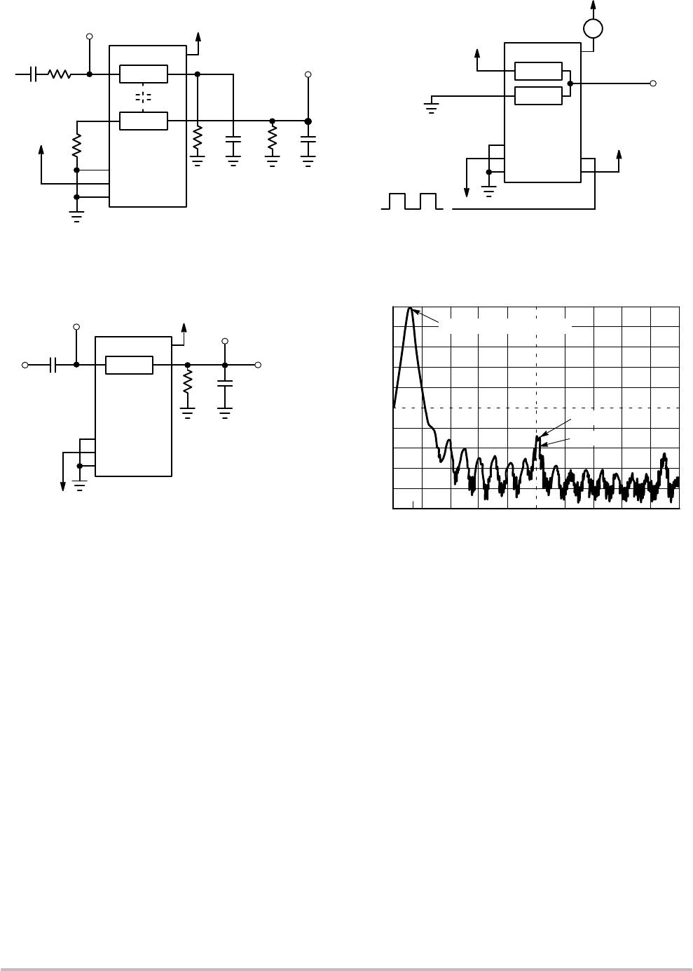
Figure 20a. Total Harmonic Distortion, Test Set−Up Figure 20b. Plot, Harmonic Distortion
0
-10
-20
-30
-40
-50
- 100
1.0 2.0 3.125
FREQUENCY (kHz)
dB
-60
-70
-80
-90
FUNDAMENTAL FREQUENCY
DEVICE
SOURCE
ON
6
7
8
16
V
EE
C
L
*
*Includes all probe and jig capacitance
OFF
R
L
R
L
V
IS
R
L
C
L
*
V
OS
f
in
0.1mF
ON/OFF
6
7
8
16
V
CC
CHANNEL SELECT
NC
COMMON O/I
OFF/ON
ANALOG I/O
V
CC
A
11
V
CC
V
EE
ON
6
7
8
16
V
CC
V
EE
0.1mF
C
L
*
f
in
R
L
TO
DISTORTION
METER
*Includes all probe and jig capacitance
V
OS
V
IS
Figure 20.
APPLICATIONS INFORMATION
The maximum analog voltage swings are determined by
the supply voltages V
CC
and V
EE
. The positive peak analog
voltage should not exceed V
CC
. Similarly, the negative peak
analog voltage should not go below V
EE
. In this example,
the difference between V
CC
and V
EE
is ten volts. Therefore,
using the configuration of Figure 21, a maximum analog
signal of ten volts peak−to−peak can be controlled. Unused
analog inputs/outputs may be left floating (i.e., not
connected). However, tying unused analog inputs and
outputs to V
CC
or GND through a low value resistor helps
minimize crosstalk and feed−through noise that may be
picked up by an unused switch.
Although used here, balanced supplies are not a
requirement. The only constraints on the power supplies are
that:
V
CC
− GND = 2 to 6 V
V
EE
− GND = 0 to −6 V
V
CC
− V
EE
= 2 to 12 V
and V
EE
≤ GND
When voltage transients above V
CC
and/or below V
EE
are
anticipated on the analog channels, external Germanium or
Schottky diodes (D
x
) are recommended as shown in
Figure 22. These diodes should be able to absorb the
maximum anticipated current surges during clipping.