XRA1202/1202P
4
8-BIT I2C/SMBUS GPIO EXPANDER WITH RESET
REV. 1.0.1
1.0 FUNCTIONAL DESCRIPTIONS
1.1 I
2
C-bus Interface
The I
2
C-bus interface is compliant with the Standard-mode and Fast-mode I
2
C-bus specifications. The I
2
C-bus
interface consists of two lines: serial data (SDA) and serial clock (SCL). In the Standard-mode, the serial clock
and serial data can go up to 100 kbps and in the Fast-mode, the serial clock and serial data can go up to 400
kbps.
The first byte sent by an I
2
C-bus master contains a start bit (SDA transition from HIGH to LOW when SCL is
HIGH), 7-bit slave address and whether it is a read or write transaction. The next byte is the sub-address that
contains the address of the register to access. The XRA120x responds to each write with an acknowledge
(SDA driven LOW by XRA1202/1202P for one clock cycle when SCL is HIGH). The last byte sent by an I
2
C-
bus master contains a stop bit (SDA transition from LOW to HIGH when SCL is HIGH). See Figures 3 - 5
below. For complete details, see the I
2
C-bus specifications.
F
IGURE
3. I
2
C S
TART
AND
S
TOP
C
ONDITIONS
F
IGURE
4. M
ASTER
W
RITES
T
O
S
LAVE
F
IGURE
5. M
ASTER
R
EADS
F
ROM
S
LAVE
SDA
SCL
S P
START condition
STOP condition
S W A A A P
SLAVE
ADDRESS
CO M M AND
BYTE
DATA
BYTE
W hite block: host to XR A120 x
G rey block: X R A 120x to host
S W A A R
SLAVE
ADDRESS
COMMAND
BYTE
White block: host to XRA120x
Grey block: XRA120x to host
AS
SLAVE
ADDRESS
nDATA A NA PLAST DATA
XRA1202/1202P
5
REV. 1.0.1
8-BIT I2C/SMBUS GPIO EXPANDER WITH RESET
1.1.1 I
2
C-bus Addressing
There could be many devices on the I
2
C-bus. To distinguish itself from the other devices on the I
2
C-bus, the
XRA1202/1202P has up to 16 I
2
C slave addresses using the A1-A0 address lines. Table 1 below shows the
different addresses that can be selected.
T
ABLE
1: I
2
C A
DDRESS
M
AP
A1 A0
I
2
C A
DDRESS
SCL GND 0x20 (0010 000X)
SCL VCC 0x22 (0010 001X)
SDA GND 0x24 (0010 010X)
SDA VCC 0x26 (0010 011X)
SCL SCL 0x30 (0011 000X)
SCL SDA 0x32 (0011 001X)
SDA SCL 0x34 (0011 010X)
SDA SDA 0x36 (0011 011X)
GND GND 0x40 (0100 000X)
GND VCC 0x42 (0100 001X)
VCC GND 0x44 (0100 010X)
VCC VCC 0x46 (0100 011X)
GND SCL 0x50 (0101 000X)
GND SDA 0x52 (0101 001X)
VCC SCL 0x54 (0101 010X)
VCC SDA 0x56 (0101 011X)
XRA1202/1202P
6
8-BIT I2C/SMBUS GPIO EXPANDER WITH RESET
REV. 1.0.1
1.1.2 I
2
C Read and Write
A read or write transaction is determined by bit-0 of the slave address. If bit-0 is ’0’, then it is a write
transaction. If bit-0 is ’1’, then it is a read transaction.
1.1.3 I
2
C Command Byte
An I
2
C command byte is sent by the I
2
C master following the slave address. The command byte indicates the
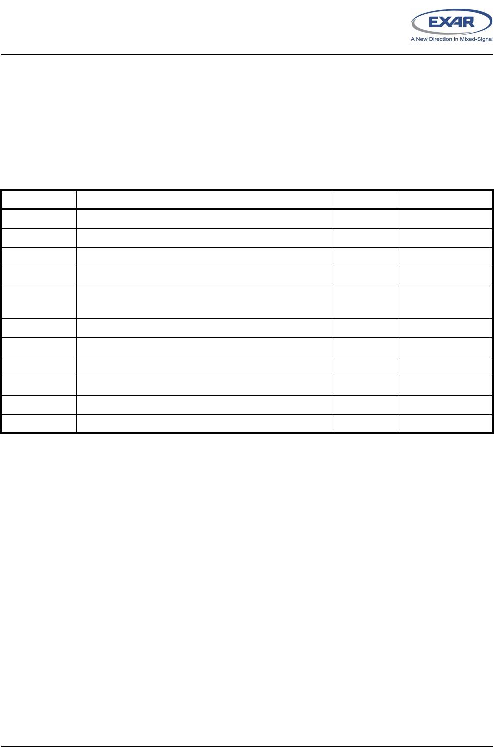
address offset of the register that will be accessed. Table 2 below lists the command bytes for each register.
T
ABLE
2: I
2
C C
OMMAND
B
YTE
(R
EGISTER
A
DDRESS
)
C
OMMAND
B
YTE
R
EGISTER
N
AME
D
ESCRIPTION
R
EAD
/W
RITE
D
EFAULT
V
ALUES
0x00 GSR - GPIO State Read-Only 0xXX
0x01 OCR - Output Control Read/Write 0xFF
0x02 PIR - Input Polarity Inversion Read/Write 0x00
0x03 GCR - GPIO Configuration Read/Write 0xFF
0x04 PUR - Input Internal Pull-up Resistor Enable/Disable Read/Write 0x00 (XRA1202)
0xFF (XRA1202P)
0x05 IER - Input Interrupt Enable Read/Write 0x00
0x06 TSCR - Output Three-State Control Read/Write 0x00
0x07 ISR - Input Interrupt Status Read 0x00
0x08 REIR - Input Rising Edge Interrupt Enable Read/Write 0x00
0x09 FEIR - Input Falling Edge Interrupt Enable Read/Write 0x00
0x0A IFR - Input Filter Enable/Disable Read/Write 0xFF

XRA1202PIL16-F

Mfr. #:
Manufacturer:
MaxLinear
Description:
Interface - I/O Expanders XRA1202PIL16-F
Lifecycle:
New from this manufacturer.
Delivery:
DHL FedEx Ups TNT EMS
Payment:
T/T Paypal Visa MoneyGram Western Union