Expand menu
Hello, Sign in
My Account
0
Cart
Home
Products
Sensors
Semiconductors
Passive Components
Connectors
Power
Electromechanical
Optoelectronics
Circuit Protection
Integrated Circuits - ICs
Main Products
Manufacturers
Blog
Services
About OMO
About Us
Contact Us
Check Stock
NCP1117DT50RKG
P1-P3
P4-P6
P7-P9
P10-P12
P13-P15
P16-P17
NCP1
1
17, NCV1
1
17
www
.onsemi.com
13
ORDERING INFORMA
TION
(continued)
Device
Shipping
†
Package
Nominal Output V
oltage
NCP1
1
17DT18RKG
1.8
DP
AK
(Pb−Free)
2500 / T
ape & Reel
NCV1
1
17DT18RKG*
1.8
DP
AK
(Pb−Free)
2500 / T
ape & Reel
NCP1
1
17DT18T5G
1.8
DP
AK
(Pb−Free)
2500 / T
ape & Reel
NCV1
1
17DT18T5G*
1.8
DP
AK
(Pb−Free)
2500 / T
ape & Reel
NCP1
1
17DT19RKG
1.9
DP
AK
(Pb−Free)
2500 / T
ape & Reel
NCP1
1
17DT20G
2.0
DP
AK
(Pb−Free)
75 Units / Rail
NCP1
1
17DT20RKG
2.0
DP
AK
(Pb−Free)
2500 / T
ape & Reel
NCV1
1
17DT20RKG*
2.0
DP
AK
(Pb−Free)
2500 / T
ape & Reel
NCP1
1
17DT25G
2.5
DP
AK
(Pb−Free)
75 Units / Rail
NCP1
1
17DT25RKG
2.5
DP
AK
(Pb−Free)
2500 / T
ape & Reel
NCV1
1
17DT25RKG*
2.5
DP
AK
(Pb−Free)
2500 / T
ape & Reel
NCP1
1
17DT25T5G
2.5
DP
AK
(Pb−Free)
2500 / T
ape & Reel
NCP1
1
17DT285G
2.85
DP
AK
(Pb−Free)
75 Units / Rail
NCP1
1
17DT285RKG
2.85
DP
AK
(Pb−Free)
2500 / T
ape & Reel
NCP1
1
17DT33G
3.3
DP
AK
(Pb−Free)
75 Units / Rail
NCP1
1
17DT33RKG
3.3
DP
AK
(Pb−Free)
2500 / T
ape & Reel
NCV1
1
17DT33T4G*
3.3
DP
AK
(Pb−Free)
2500 / T
ape & Reel
NCP1
1
17DT33T5G
3.3
DP
AK
(Pb−Free)
2500 / T
ape & Reel
NCV1
1
17DT33T5G*
3.3
DP
AK
(Pb−Free)
2500 / T
ape & Reel
NCP1
1
17DT50G
5.0
DP
AK
(Pb−Free)
75 Units / Rail
NCP1
1
17DT50RKG
5.0
DP
AK
(Pb−Free)
2500 / T
ape & Reel
NCV1
1
17DT50RKG*
5.0
DP
AK
(Pb−Free)
2500 / T
ape & Reel
NCP1
1
17DT12G
12
DP
AK
(Pb−Free)
75 Units / Rail
NCP1
1
17DT12RKG
12
DP
AK
(Pb−Free)
2500 / T
ape & Reel
NCV1
1
17DT12RKG*
12
DP
AK
(Pb−Free)
2500 / T
ape & Reel
†
For information on tape and reel specifications, including part orientation and tape sizes, please refer to our T
ape and Reel
Packaging
Specifications Brochure, BRD801
1/D.
*NCV Prefix for Automotive and Other Applications Requiring Unique Site and Control Change Requirements; AEC−Q100 Qualified and
PP
AP Capable
NCP1
1
17, NCV1
1
17
www
.onsemi.com
14
1
17AJG
AL
YWW
17−15G
AL
YWW
17−18G
AL
YWW
1
17−2G
AL
YWW
17−25G
AL
YWW
17285G
AL
YWW
17−33G
AL
YWW
1
17−5G
AL
YWW
17−12G
AL
YWW
AY
W
1
17−A
G
G
1
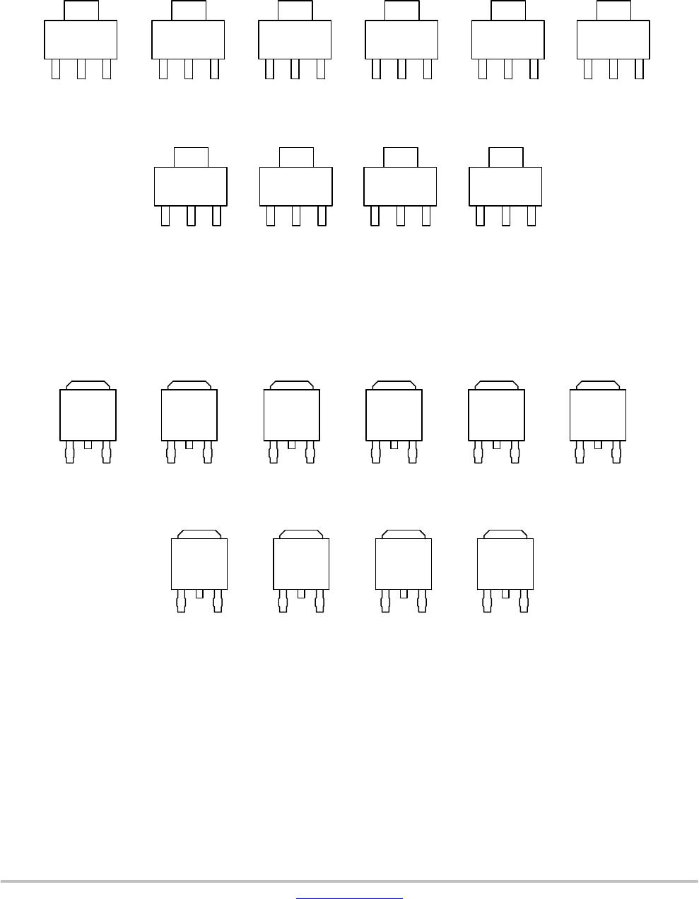
SOT−223
ST SUFFIX
CASE 318H
A
= Assembly Location
L
= W
afer Lot
Y
= Y
ear
WW
, W
= W
ork Week
G
or G
= Pb−Free Package
MARKING DIAGRAMS − NCP PREFIX
DP
AK
DT SUFFIX
CASE 369C
23
1
2
31
2
31
2
31
2
31
2
3
1
2
31
2
31
2
31
2
3
Adjustable
1.5 V
1.8 V
2.0 V
2.5 V
2.85 V
3.3 V
5.0 V
12 V
Adjustable
1.5 V
1.8 V
2.0 V
2.5 V
2.85 V
3.3 V
5.0 V
12 V
(Note: Microdot may be in either location)
AY
W
17−15
G
G
1
23
AY
W
17−18
G
G
1
23
AY
W
1
17−2
G
G
1
23
AY
W
17−25
G
G
1
23
AY
W
7−285
G
G
1
23
AY
W
17−33
G
G
1
23
AY
W
1
17−5
G
G
1
23
AY
W
17−12
G
G
1
23
1.9 V
AY
W
17−19
G
G
1
23
17−19G
AL
YWW
1
2
3
1.9 V
NCP1
1
17, NCV1
1
17
www
.onsemi.com
15
17AJVG
AL
YWW
1715VG
AL
YWW
1718VG
AL
YWW
1
172VG
AL
YWW
1725VG
AL
YWW
1733VG
AL
YWW
1
175VG
AL
YWW
AY
W
1
17A
V
G
G
1
SOT−223
ST SUFFIX
CASE 318H
A
= Assembly Location
L
= W
afer Lot
Y
= Y
ear
WW
, W
= W
ork Week
G
or G
= Pb−Free Package
MARKING DIAGRAMS − NCV PREFIX
DP
AK
DT SUFFIX
CASE 369C
23
1
2
31
2
31
2
31
2
3
1
2
3
1
2
31
2
3
Adjustable
1.5 V
2.0 V
2.5 V
3.3 V
5.0 V
Adjustable
1.5 V
1.8 V
2.0 V
2.5 V
3.3 V
5.0 V
(Note: Microdot may be in either location)
AY
W
1715V
G
G
1
23
AY
W
1
172V
G
G
1
23
AY
W
1725V
G
G
1
23
AY
W
1733V
G
G
1
23
AY
W
1750V
G
G
1
23
1.8 V
AY
W
1718V
G
G
1
23
12 V
AY
W
1712V
G
G
1
23
1712VG
AL
YWW
1
2
3
12 V
P1-P3
P4-P6
P7-P9
P10-P12
P13-P15
P16-P17
NCP1117DT50RKG
Mfr. #:
Buy NCP1117DT50RKG
Manufacturer:
ON Semiconductor
Description:
LDO Voltage Regulators 5.0V 1A Positive
Lifecycle:
New from this manufacturer.
Delivery:
DHL
FedEx
Ups
TNT
EMS
Payment:
T/T
Paypal
Visa
MoneyGram
Western
Union
Products related to this Datasheet
NCV1117DT20RKG
NCP1117DTAT5G
NCP1117DT25T5G
NCP1117DT50G
NCP1117DT33G
NCP1117ST18T3G
NCP1117ST12T3G
NCP1117DTARKG
NCP1117DTAG
NCP1117DT12G
NCV1117DTARKG
NCP1117DT25RKG
NCP1117ST20T3G
NCV1117ST20T3G
NCP1117DT25G
NCV1117DT18RKG
NCP1117DT20G
NCP1117DT15G
NCP1117DT18G
NCP1117DT285G
NCV1117DT33T4G
NCP1117DT285RKG
NCP1117ST33T3G
NCP1117DT33T5G
NCV1117STAT3G
NCV1117ST25T3G
NCP1117DT15RKG
NCP1117DT18RKG
NCP1117DT12RKG
NCP1117DT18T5G
NCP1117ST15T3G
NCP1117DT20RKG
NCV1117ST15T3G
NCV1117DT25RKG
NCV1117DT15RKG
NCV1117DT18T5G