NCP1117, NCV1117
www.onsemi.com
4
ELECTRICAL CHARACTERISTICS (continued)
(C
in
= 10 mF, C
out
= 10 mF, for typical value T
A
= 25°C, for min and max values T
A
is the operating ambient temperature range that applies
unless otherwise noted.) (Note 4)
Characteristic UnitMaxTypMinSymbol
Quiescent Current
1.5 V (V
in
= 11.5 V)
1.8 V (V
in
= 11.8 V)
1.9 V (V
in
= 11.9 V)
2.0 V (V
in
= 12 V)
2.5 V (V
in
= 10 V)
2.85 V (V
in
= 10 V)
3.3 V (V
in
= 15 V)
5.0 V (V
in
= 15 V)
12 V (V
in
= 20 V)
I
Q
3.6
4.2
4.3
4.5
5.2
5.5
6.0
6.0
6.0
10
10
10
10
10
10
10
10
10
mA
Thermal Regulation (T
A
= 25°C, 30 ms Pulse) 0.01 0.1 %/W
Ripple Rejection (V
in
−V
out
= 6.4 V, I
out
= 500 mA, 10 V
pp
120 Hz Sinewave)
Adjustable
1.5 V
1.8 V
1.9 V
2.0 V
2.5 V
2.85 V
3.3 V
5.0 V
12 V
RR
67
66
66
66
64
62
62
60
57
50
73
72
70
72
70
68
68
64
61
54
dB
Adjustment Pin Current (V
in
= 11.25 V, I
out
= 800 mA) I
adj
52 120
mA
Adjust Pin Current Change
(V
in
−V
out
= 1.4 V to 10 V, I
out
= 10 mA to 800 mA)
DI
adj
0.4 5.0
mA
Temperature Stability S
T
0.5 %
Long Term Stability (T
A
= 25°C, 1000 Hrs End Point Measurement) S
t
0.3 %
RMS Output Noise (f = 10 Hz to 10 kHz) N 0.003 %V
out
Product parametric performance is indicated in the Electrical Characteristics for the listed test conditions, unless otherwise noted. Product
performance may not be indicated by the Electrical Characteristics if operated under different conditions.
4. NCP1117: T
low
= 0°C , T
high
= 125°C
NCV1117: T
low
= −40°C, T
high
= 125°C
5. Low duty cycle pulse techniques are used during testing to maintain the junction temperature as close to ambient as possible.
6. The regulator output current must not exceed 1.0 A with V
in
greater than 12 V.
NCP1117, NCV1117
www.onsemi.com
5
V
in
− V
out
, DROPOUT VOLTAGE (V)
T
A
, AMBIENT TEMPERATURE (°C)
I
adj
, ADJUST PIN CURRENT (
m
A)
I
out
= 10 mA
0
20
40
60
80
100
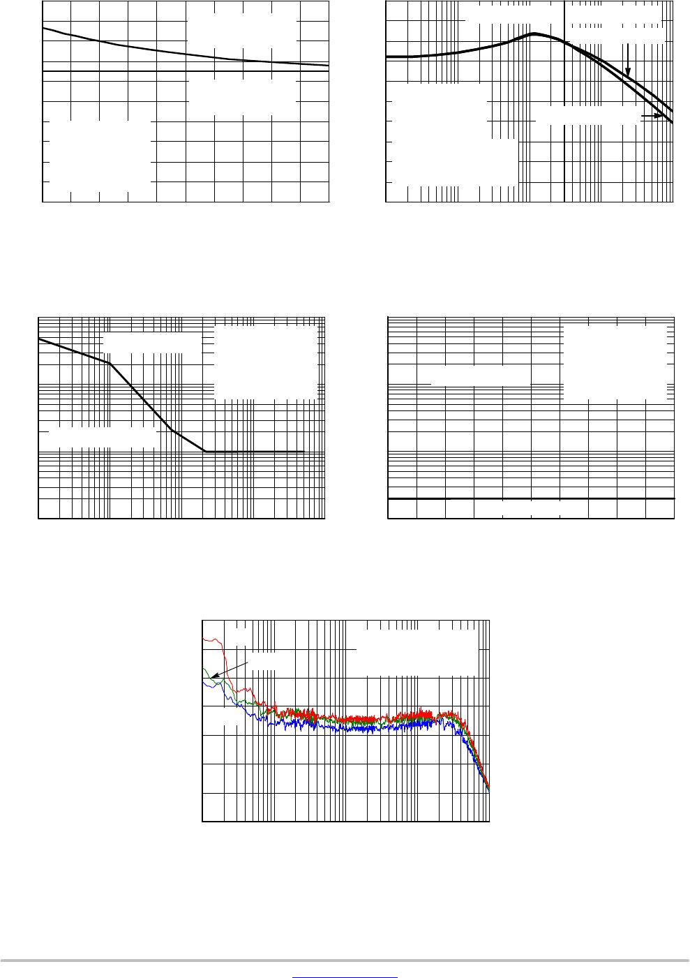
Figure 4. Output Voltage Change
vs. Temperature
Figure 5. Dropout Voltage
vs. Output Current
Figure 6. Output Short Circuit Current
vs. Differential Voltage
Figure 7. Output Short Circuit Current
vs. Temperature
Figure 8. Adjust Pin Current
vs. Temperature
Figure 9. Quiescent Current Change
vs. Temperature
0
0.5
1.0
1.5
2.0
0 2 4 6 8 101214161820
Load pulsed at 1.0% duty cycle
V
in
− V
out
, VOLTAGE DIFFERENTIAL (V)
I
out
, OUTPUT CURRENT (A)
T
J
= 25°C
0
0.2
0.4
0.6
0.8
1.0
1.2
1.4
0 200 400 600 800 100
0
Load pulsed at 1.0% duty cycle
I
out
, OUTPUT CURRENT (mA)
T
J
= −40°C
T
J
= 25°C
T
J
= 125°C
V
out
, OUTPUT VOLTAGE CHANGE (%)
−2.0
−1.5
−1.0
−0.5
0
0.5
1.0
1.5
2.0
−50 −25 0 25 50 75 100 125
150
T
A
, AMBIENT TEMPERATURE (°C)
V
in
= V
out
+ 3.0 V
I
out
= 10 mA
Adj, 1.5 V,
1.8 V, 2.0 V,
2.5 V
2.85 V, 3.3 V,
5.0 V, 12.0 V
1.0
1.2
1.4
1.6
1.8
2.0
−50 −25 0 25 50 75 100 125 15
0
−20
−15
−10
−5.0
0
5.0
10
−50 −25 0 25 50 75 100 125 15
0
T
A
, AMBIENT TEMPERATURE (°C)
I
out
, OUTPUT CURRENT (A)
V
in
= 5.0 V
Load pulsed at 1.0% duty cycle
T
A
, AMBIENT TEMPERATURE (°C)
I
Q,
QUIESCENT CURRENT CHANGE (%)
−50 −25 0 25 50 75 100 125 150
NCP1117, NCV1117
www.onsemi.com
6
0
20
40
60
80
100
10 100 1.0 k 10 k 100
k
0
20
40
60
80
100
0 200 400 600 800 1000
I
out
, OUTPUT CURRENT (mA)
RR, RIPPLE REJECTION (dB)
f
ripple
= 20 kHz
V
ripple
v 0.5 V
P−P
V
out
= 5.0 V
V
in
− V
out
= 3.0 V
C
out
= 10 mF
C
adj
= 25 mF
T
A
= 25°C
f
ripple
, RIPPLE FREQUENCY (Hz)
RR, RIPPLE REJECTION (dB)
V
out
= 5.0 V
V
in
− V
out
= 3.0 V
I
out
= 0.5 A
C
out
= 10 mF
C
adj
= 25 mF, f > 60 Hz
V
ripple
v 3.0 V
P−P
V
ripple
v 0.5 V
P−P
V
in
− V
out
w 3.0 V
Figure 10. NCP1117XTA Ripple Rejection
vs. Output Current
Figure 11. NCP1117XTA Ripple Rejection
vs. Frequency
Figure 12. Output Capacitance vs. ESR
Figure 13. Typical ESR vs. Output Current
f
ripple
= 120 Hz
V
ripple
v 3.0 V
P−P
V
in
− V
out
w V
dropout
C
adj
= 200 mF, f v 60 Hz
T
A
= 25°C
0.1
1
10
100
0.001 0.01 0.1 1 10
ESR, EQUIVALENT SERIES RESISTANCE (W)
OUTPUT CAPACITANCE (
m
F)
V
in
= 3.0 V
V
out
= 1.25 V
I
load
= 5 mA − 1 A
C
in
= 10 mF MLCC
T
J
= 25°C
Region of Instability
Region of Stability
0.01
0.1
1
10
0 100 500 900 100
0
I
out
, OUTPUT CURRENT (mA)
ESR, EQUIVALENT SERIES RESISTANCE (W)
V
in
= 3.0 V
V
out
= 1.25 V
C
in
= 10 mF MLCC
C
out
= 10 mF
T
J
= 25°C
Region of Instability
Region of Stability
200 600300 700400 800
0
50E−9
100E−9
150E−9
200E−9
250E−9
10 100 1.0 k 10 k 100 k
FREQUENCY (Hz)
V/sqrt (Hz)
C
in
= 10 mF Tantalum
C
out
= 10 mF Tantalum
V
in
− V
out
= 3.0 V
Figure 14. Output Spectral Noise Density vs.
Frequency, V
out
= 1V5
300E−9
350E−9
1 A
0.5 A
0.1 A

NCP1117DT50RKG

Mfr. #:
Manufacturer:
ON Semiconductor
Description:
LDO Voltage Regulators 5.0V 1A Positive
Lifecycle:
New from this manufacturer.
Delivery:
DHL FedEx Ups TNT EMS
Payment:
T/T Paypal Visa MoneyGram Western Union