NCP1117, NCV1117
www.onsemi.com
9
APPLICATIONS INFORMATION
Introduction
The NCP1117 features a significant reduction in dropout
voltage along with enhanced output voltage accuracy and
temperature stability when compared to older industry
standard three−terminal adjustable regulators. These
devices contain output current limiting, safe operating area
compensation and thermal shutdown protection making
them designer friendly for powering numerous consumer
and industrial products. The NCP1117 series is pin
compatible with the older LM317 and its derivative device
types.
Output Voltage
The typical application circuits for the fixed and
adjustable output regulators are shown in Figures 23 and 24.
The adjustable devices are floating voltage regulators. They
develop and maintain the nominal 1.25 V reference voltage
between the output and adjust pins. The reference voltage is
programmed to a constant current source by resistor R1, and
this current flows through R2 to ground to set the output
voltage. The programmed current level is usually selected to
be greater than the specified 5.0 mA minimum that is
required for regulation. Since the adjust pin current, I
adj
, is
significantly lower and constant with respect to the
programmed load current, it generates a small output
voltage error that can usually be ignored. For the fixed
output devices R1 and R2 are included within the device and
the ground current I
gnd
, ranges from 3.0 mA to 5.0 mA
depending upon the output voltage.
External Capacitors
Input bypass capacitor C
in
may be required for regulator
stability if the device is located more than a few inches from
the power source. This capacitor will reduce the circuit’s
sensitivity when powered from a complex source impedance
and significantly enhance the output transient response. The
input bypass capacitor should be mounted with the shortest
possible track length directly across the regulator’s input
and ground terminals. A 10 mF ceramic or tantalum
capacitor should be adequate for most applications.
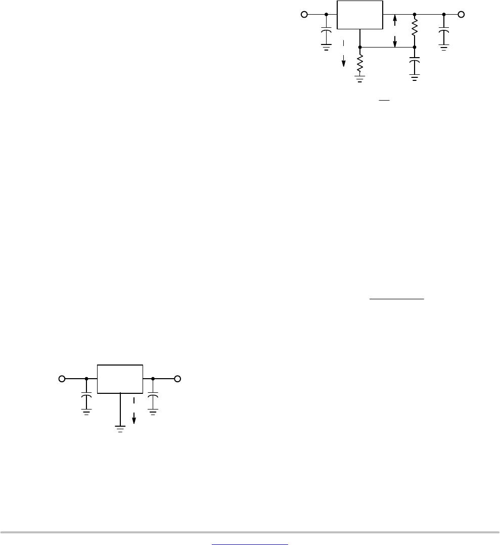
Figure 23. Fixed Output Regulator
1
2
Output
3
Input
NCP1117
XTXX
++
C
out
C
in
I
gnd
Frequency compensation for the regulator is provided by
capacitor C
out
and its use is mandatory to ensure output
stability. A minimum capacitance value of 4.7 mF with an
equivalent series resistance (ESR) that is within the limits of
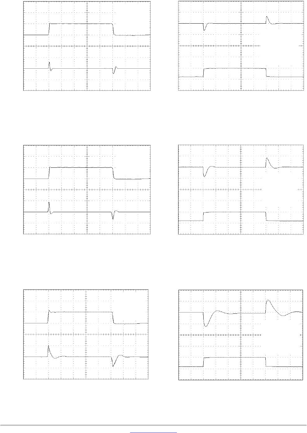
33 mW (typ) to 2.2 W is required. See Figures 12 and 13. The
capacitor type can be ceramic, tantalum, or aluminum
electrolytic as long as it meets the minimum capacitance
value and ESR limits over the circuit’s entire operating
temperature range. Higher values of output capacitance can
be used to enhance loop stability and transient response with
the additional benefit of reducing output noise.
Figure 24. Adjustable Output Regulator
1
2
Output
3
Input
NCP1117
XTA
++
C
out
C
in
I
adj
R2
+
C
adj
V
ref
R1
V
out
+ V
ref
ǒ
1 )
R2
R1
Ǔ
) I
adj
R2
The output ripple will increase linearly for fixed and
adjustable devices as the ratio of output voltage to the
reference voltage increases. For example, with a 12 V
regulator, the output ripple will increase by 12 V/1.25 V or
9.6 and the ripple rejection will decrease by 20 log of this
ratio or 19.6 dB. The loss of ripple rejection can be restored
to the values shown with the addition of bypass capacitor
C
adj
, shown in Figure 24. The reactance of C
adj
at the ripple
frequency must be less than the resistance of R1. The value
of R1 can be selected to provide the minimum required load
current to maintain regulation and is usually in the range of
100 W to 200 W.
C
adj
u
1
2 p f
ripple
R1
The minimum required capacitance can be calculated
from the above formula. When using the device in an
application that is powered from the AC line via a
transformer and a full wave bridge, the value for C
adj
is:
f
ripple +
120 Hz, R1 + 120 W, then C
adj
u 11.1 mF
The value for C
adj
is significantly reduced in applications
where the input ripple frequency is high. If used as a post
regulator in a switching converter under the following
conditions:
f
ripple
+ 50 kHz, R1 + 120 W, then C
adj
u 0.027 mF
Figures 10 and 11 shows the level of ripple rejection that
is obtainable with the adjust pin properly bypassed.