2.7 V, 800 μA, 80 MHz
Rail-to-Rail I/O Amplifiers
Data Sheet
AD8031/AD8032
Rev. G Document Feedback
Information furnished by Analog Devices is believed to be accurate and reliable. However, no
responsibility is assumed by Analog Devices for its use, nor for any infringements of patents or other
rights of third parties that may result from its use. Specifications subject to change without notice. No
license is granted by implication or otherwise under any patent or patent rights of Analog Devices.
Trademarks and registered trademarks are the property of their respective owners.
One Technology Way, P.O. Box 9106, Norwood, MA 02062-9106, U.S.A.
Tel: 781.329.4700 ©2014 Analog Devices, Inc. All rights reserved.
Technical Support www.analog.com
FEATURES
Low power
Supply current 800 μA/amplifier
Fully specified at +2.7 V, +5 V, and ±5 V supplies
High speed and fast settling on 5 V
80 MHz, −3 dB bandwidth (G = +1)
30 V/μs slew rate
125 ns settling time to 0.1%
Rail-to-rail input and output
No phase reversal with input 0.5 V beyond supplies
Input CMVR extends beyond rails by 200 mV
Output swing to within 20 mV of either rail
Low distortion
−62 dB @ 1 MHz, V
O
= 2 V p-p
−86 dB @ 100 kHz, V
O
= 4.6 V p-p
Output current: 15 mA
High grade option: V
OS
(maximum) = 1.5 mV
APPLICATIONS
High speed, battery-operated systems
High component density systems
Portable test instruments
A/D buffers
Active filters
High speed, set-and-demand amplifiers
GENERAL DESCRIPTION
The AD8031 (single) and AD8032 (dual) single-supply, voltage
feedback amplifiers feature high speed performance with
80 MHz of small signal bandwidth, 30 V/μs slew rate, and 125 ns
settling time. This performance is possible while consuming less
than 4.0 mW of power from a single 5 V supply. These features
increase the operation time of high speed, battery-powered
systems without compromising dynamic performance.
The products have true single-supply capability with rail-to-rail
input and output characteristics and are specified for +2.7 V, +5 V,
and ±5 V supplies. The input voltage range can extend to 500 mV
beyond each rail. The output voltage swings to within 20 mV of
each rail providing the maximum output dynamic range.
The AD8031/AD8032 also offer excellent signal quality for only
800 μA of supply current per amplifier; THD is −62 dBc with a
2 V p-p, 1 MHz output signal, and –86 dBc for a 100 kHz,
4.6 V p-p signal on +5 V supply. The low distortion and fast
settling time make them ideal as buffers to single-supply ADCs.
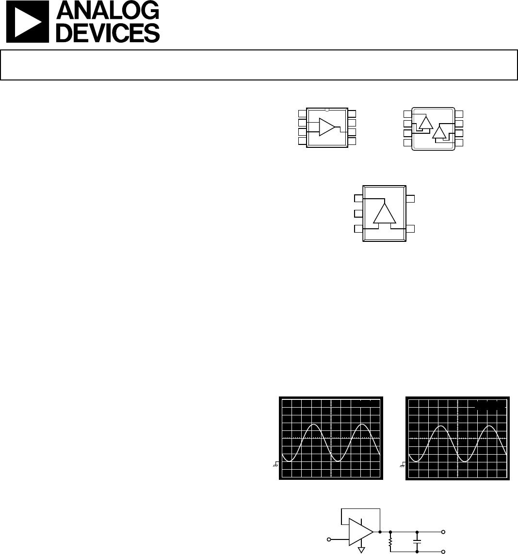
CONNECTION DIAGRAMS
NC
1
–IN
2
+IN
3
V
S
4
NC
8
+V
S
7
OUT
6
NC
5
NC = NO CONNECT
AD8031
+
01056-001
OUT1
1
–IN1
2
+IN1
3
–V
S
4
+V
S
8
OUT2
7
–IN2
6
+IN2
5
AD8032
+–
+–
01056-002
Figure 1. 8-Lead PDIP (N) and
SOIC_N (R)
Figure 2. 8-Lead PDIP (N),
SOIC_N (R), and MSOP (RM)
V
OUT
1
+IN
3
–V
S
2
+V
S
5
–IN
4
AD8031
+
01056-003
Figure 3. 5-Lead SOT-23 (RJ-5)
Operating on supplies from +2.7 V to +12 V and dual supplies
up to ±6 V, the AD8031/AD8032 are ideal for a wide range of
applications, from battery-operated systems with large bandwidth
requirements to high speed systems where component density
requires lower power dissipation. The AD8031/AD8032 are
available in 8-lead PDIP and 8-lead SOIC_N packages and
operate over the industrial temperature range of −40°C to
+85°C. The AD8031A is also available in the space-saving
5-lead SOT-23 package, and the AD8032A is available in an
8-lead MSOP package.
2µs/DIV
1V/DIV
V
IN
=4.85Vp-p
01056-004
1V/DI
V
2µs/DIV
V
OUT
=4.65Vp-p
G=+1
01056-005
Figure 4. Input V
IN
Figure 5. Output V
OUT
V
IN
+5V
1k 1.7pF
+2.5V
V
OUT
+
01056-006
Figure 6. Rail-to-Rail Performance at 100 kHz
AD8031/AD8032 Data Sheet
Rev. G | Page 2 of 20
TABLE OF CONTENTS
Features .............................................................................................. 1
Applications ....................................................................................... 1
General Description ......................................................................... 1
Connection Diagrams ...................................................................... 1
Revision History ............................................................................... 2
Specifications ..................................................................................... 3
+2.7 V Supply ................................................................................ 3
+5 V Supply ................................................................................... 4
±5 V Supply ................................................................................... 5
Absolute Maximum Ratings ............................................................ 6
Maximum Power Dissipation ..................................................... 6
ESD Caution .................................................................................. 6
Typical Performance Characteristics ............................................. 7
Theory of Operation ...................................................................... 13
Input Stage Operation ................................................................ 13
Overdriving the Input Stage...................................................... 13
Output Stage, Open-Loop Gain and Distortion vs. Clearance
from Power Supply ..................................................................... 14
Output Overdrive Recovery ...................................................... 14
Driving Capacitive Loads .......................................................... 15
Applications ..................................................................................... 16
A 2 MHz Single-Supply, Biquad Band-Pass Filter ................. 16
High Performance, Single-Supply Line Driver........................... 16
Outline Dimensions ....................................................................... 18
Ordering Guide .......................................................................... 20
REVISION HISTORY
3/14Rev. F to Rev. G
Changes to Second Paragraph of Theory of Operation Section ... 13
Changes to Ordering Guide .......................................................... 20
8/13Rev. E to Rev. F
Changed Input Current Noise at f = 100 kHz from 2.4 pA/√Hz
to 0.4 pA/√Hz (Throughout) .......................................................... 3
6/13Rev. D to Rev. E
Changes to DC Performance Parameter, Table 1 ......................... 3
Updated Outline Dimensions ....................................................... 19
Changes to Ordering Guide .......................................................... 20
11/08Rev. C to Rev. D
Change to Table 3 Column Heading .............................................. 5
Change to Ordering Guide ............................................................ 20
7/06Rev. B to Rev. C
Updated Format .................................................................. Universal
Updated Outline Dimensions ....................................................... 18
Change to Ordering Guide ............................................................ 20
9/99Rev. A to Rev. B
Data Sheet AD8031/AD8032
Rev. G | Page 3 of 20
SPECIFICATIONS
+2.7 V SUPPLY
@ T
A
= 25°C, V
S
= 2.7 V, R
L
= 1 kΩ to 1.35 V, R
F
= 2.5 kΩ, unless otherwise noted.
Table 1.
AD8031A/AD8032A AD8031B/AD8032B
Parameter Conditions Min Typ Max Min Typ Max Unit
DYNAMIC PERFORMANCE
3 dB Small Signal Bandwidth
G = +1, V
O
< 0.4 V p-p
54
80
80
MHz
Slew Rate G = 1, V
O
= 2 V step 25 30 25 30 V/µs
Settling Time to 0.1% G = −1, V
O
= 2 V step, C
L
= 10 pF 125 125 ns
DISTORTION/NOISE PERFORMANCE
Total Harmonic Distortion f
C
= 1 MHz, V
O
= 2 V p-p, G = +2 62 −62 dBc
f
C
= 100 kHz, V
O
= 2 V p-p, G = +2 86 −86 dBc
Input Voltage Noise f = 1 kHz 15 15 nV/√Hz
Input Current Noise f = 100 kHz 0.4 0.4 pA/√Hz
f = 1 kHz 5 5 pA/√Hz
Crosstalk (AD8032 Only) f = 5 MHz 60 −60 dB
DC PERFORMANCE
Input Offset Voltage
V
CM
= V
CC
/2; V
OUT
= 1.35 V
±1
±6
±0.5
±1.5
mV
T
MIN
to T
MAX
±6 ±10 ±1.6 ±2.5 mV
Offset Drift V
CM
= V
CC
/2; V
OUT
= 1.35 V 10 10 µVC
Input Bias Current V
CM
= V
CC
/2; V
OUT
= 1.35 V 0.45 2 0.45 2 µA
T
MIN
to T
MAX
2.2 2.2 µA
Input Offset Current 50 500 50 500 nA
Open-Loop Gain V
CM
= V
CC
/2; V
OUT
= 0.35 V to 2.35 V 76 80 76 80 dB
T
MIN
to T
MAX
74 74 dB
INPUT CHARACTERISTICS
Common-Mode Input Resistance 40 40
Differential Input Resistance 280 280
Input Capacitance 1.6 1.6 pF
Input Voltage Range −0.5 to
+3.2
−0.5 to
+3.2
V
Input Common-Mode Voltage Range −0.2 to
+2.9
0.2 to
+2.9
V
Common-Mode Rejection Ratio V
CM
= 0 V to 2.7 V 46 64 46 64 dB
V
CM
= 0 V to 1.55 V 58 74 58 74 dB
Differential Input Voltage 3.4 3.4 V
OUTPUT CHARACTERISTICS
Output Voltage Swing Low R
L
= 10 kΩ 0.05 0.02 0.05 0.02 V
Output Voltage Swing High 2.6 2.68 2.6 2.68 V
Output Voltage Swing Low
R
L
= 1 kΩ
0.15
0.08
0.08
V
Output Voltage Swing High 2.55 2.6 2.55 2.6 V
Output Current 15 15 mA
Short Circuit Current Sourcing 21 21 mA
Sinking −34 34 mA
Capacitive Load Drive G = +2 (See Figure 46) 15 15 pF
POWER SUPPLY
Operating Range 2.7 12 2.7 12 V
Quiescent Current per Amplifier 750 1250 750 1250 μA
Power Supply Rejection Ratio
V
S
− = 0 V to −1 V or
V
S
+ = +2.7 V to +3.7 V
75
86
86
dB

AD8032BRZ

Mfr. #:
Manufacturer:
Analog Devices Inc.
Description:
Operational Amplifiers - Op Amps 2.7V 800uA 80Mhz RRIO Dual
Lifecycle:
New from this manufacturer.
Delivery:
DHL FedEx Ups TNT EMS
Payment:
T/T Paypal Visa MoneyGram Western Union