Data Sheet AD8031/AD8032
Rev. G | Page 13 of 20
THEORY OF OPERATION
The AD8031/AD8032 are single and dual versions of high
speed, low power, voltage feedback amplifiers featuring an
innovative architecture that maximizes the dynamic range
capability on the inputs and outputs. The linear input common-
mode range exceeds either supply voltage by 200 mV, and the
amplifiers show no phase reversal up to 500 mV beyond supply.
The output swings to within 20 mV of either supply when
driving a light load; 300 mV when driving up to 5 mA.
Fabricated on Analog Devices, Inc. eXtra Fast Complementary
Bipolar (XFCB) process, the amplifier provides an impressive
80 MHz bandwidth when used as a follower and a 30 V/µs slew
rate at only 800 µA supply current. Careful design allows the
amplifier to operate with a supply voltage as low as 2.7 V.
INPUT STAGE OPERATION
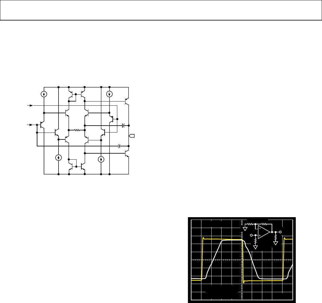
A simplified schematic of the input stage appears in Figure 43.
For common-mode voltages up to 1.1 V within the positive
supply (0 V to 3.9 V on a single 5 V supply), tail current I2
flows through the PNP differential pair, Q13 and Q17. Q5 is cut
off; no bias current is routed to the parallel NPN differential
pair, Q2 and Q3. As the common-mode voltage is driven within
1.1 V of the positive supply, Q5 turns on and routes the tail
current away from the PNP pair and to the NPN pair. During
this transition region, the input current of the amplifier changes
magnitude and direction. Reusing the same tail current ensures
that the input stage has the same transconductance, which
determines the gain and bandwidth of the amplifier, in both
regions of operation.
Switching to the NPN pair as the common-mode voltage is
driven beyond 1 V within the positive supply allows the amplifier
to provide useful operation for signals at either end of the
supply voltage range and eliminates the possibility of phase
reversal for input signals up to 500 mV beyond either power
supply. Offset voltage also changes to reflect the offset of the
input pair in control. The transition region is small, approximately
180 mV. These sudden changes in the dc parameters of the
input stage can produce glitches that adversely affect distortion.
OVERDRIVING THE INPUT STAGE
Sustained input differential voltages greater than 3.4 V should
be avoided as the input transistors can be damaged. Input clamp
diodes are recommended if the possibility of this condition
exists.
The voltages at the collectors of the input pairs are set to
200 mV from the power supply rails. This allows the amplifier
to remain in linear operation for input voltages up to 500 mV
beyond the supply voltages. Driving the input common-mode
voltage beyond that point will forward bias the collector junction of
the input transistor, resulting in phase reversal. Sustaining this
condition for any length of time should be avoided because it is
easy to exceed the maximum allowed input differential voltage
when the amplifier is in phase reversal.
Q3
Q2
Q13
Q17
Q6
Q8
Q10
4
Q14
4
1
1
Q7
Q15
1
Q11
4
1
4
Q16
Q18
Q4
V
CC
V
IN
V
IP
Q5
Q9
V
EE
OUTPUT STAGE,
C
OMMON-MOD
E
FEEDBACK
R4
2k
R2
2k
R1
2k
I3
25µA
I4
25µA
R3
2k
I1
5µA
I
2
90µA
1.1V
R5
50k
R6
850
R7
850
R8
850
R9
850
01056-043
Figure 43. Simplified Schematic of AD8031 Input Stage
AD8031/AD8032 Data Sheet
Rev. G | Page 14 of 20
OUTPUT STAGE, OPEN-LOOP GAIN AND
DISTORTION vs. CLEARANCE FROM POWER
SUPPLY
The AD8031 features a rail-to-rail output stage. The output
transistors operate as common-emitter amplifiers, providing the
output drive current as well as a large portion of the amplifier’s
open-loop gain.
DIFFERENTIAL
DR
I
VE
FROM
I
NP
U
T S
TA
G
E
Q37
Q47
Q2
1
Q2
0
Q51
Q27
Q68
Q
44
Q
4
2
Q4
8
Q49
Q
50
Q
43
V
O
U
T
Q38
I
1
25µA
I2
25µA
C
9
5pF
C5
1.
5p
F
I
5
25
µA
I4
25µA
R
2
9
300
+
+
01056-044
Figure 44. Output Stage Simplified Schematic
The output voltage limit depends on how much current the
output transistors are required to source or sink. For applications
with low drive requirements (for instance, a unity gain follower
driving another amplifier input), the AD8031 typically swings
within 20 mV of either voltage supply. As the required current
load increases, the saturation output voltage increases linearly as
I
LOAD
× R
C
where:
I
LOAD
is the required load current.
R
C
is the output transistor collector resistance.
For the AD8031, the collector resistances for both output
transistors are typically 25 Ω. As the current load exceeds the
rated output current of 15 mA, the amount of base drive current
required to drive the output transistor into saturation reaches its
limit, and the amplifier’s output swing rapidly decreases.
The open-loop gain of the AD8031 decreases approximately
linearly with load resistance and depends on the output voltage.
Open-loop gain stays constant to within 250 mV of the positive
power supply, 150 mV of the negative power supply, and then
decreases as the output transistors are driven further into
saturation.
The distortion performance of the AD8031/AD8032 amplifiers
differs from conventional amplifiers. Typically, the distortion
performance of the amplifier degrades as the output voltage
amplitude increases.
Used as a unity gain follower, the output of the AD8031/
AD8032 exhibits more distortion in the peak output voltage
region around V
CC
0.7 V. This unusual distortion characteristic is
caused by the input stage architecture and is discussed in detail
in the Input Stage Operation section,
OUTPUT OVERDRIVE RECOVERY
Output overdrive of an amplifier occurs when the amplifier
attempts to drive the output voltage to a level outside its normal
range. After the overdrive condition is removed, the amplifier
must recover to normal operation in a reasonable amount of
time. As shown in Figure 45, the AD8031/AD8032 recover
within 100 ns from negative overdrive and within 80 ns from
positive overdrive.
R
L
50
V
IN
V
OU
T
100
ns1V
V
S
= ±2.5V
V
I
N
= ±2.
5V
R
L
=
1kT
O GND
R
F
= R
G
= 2k
R
G
R
F
01056-045
Figure 45. Overdrive Recovery
Data Sheet AD8031/AD8032
Rev. G | Page 15 of 20
DRIVING CAPACITIVE LOADS
Capacitive loads interact with an op amps output impedance to
create an extra delay in the feedback path. This reduces circuit
stability and can cause unwanted ringing and oscillation. A
given value of capacitance causes much less ringing when the
amplifier is used with a higher noise gain.
The capacitive load drive of the AD8031/AD8032 can be
increased by adding a low valued resistor in series with the
capacitive load. Introducing a series resistor tends to isolate the
capacitive load from the feedback loop, thereby diminishing its
influence. Figure 46 shows the effects of a series resistor on the
capacitive drive for varying voltage gains. As the closed-loop
gain is increased, the larger phase margin allows for larger
capacitive loads with less overshoot. Adding a series resistor at
lower closed-loop gains accomplishes the same effect. For large
capacitive loads, the frequency response of the amplifier is
dominated by the roll-off of the series resistor and capacitive load.
1000
10
100
CAPACITIVE LOAD (pF)
CLOSED-LOOP GAIN (V/V)
1
0 1 2 3 4 5
R
S
= 5
R
S
= 0
R
S
= 20
R
S
= 20
R
S
= 0, 5
V
S
= 5V
200mV STEP
WITH 30% OVERSHOOT
R
G
R
F
R
S
C
L
V
OUT
01056-046
Figure 46. Capacitive Load Drive vs. Closed-Loop Gain

AD8032BRZ

Mfr. #:
Manufacturer:
Analog Devices Inc.
Description:
Operational Amplifiers - Op Amps 2.7V 800uA 80Mhz RRIO Dual
Lifecycle:
New from this manufacturer.
Delivery:
DHL FedEx Ups TNT EMS
Payment:
T/T Paypal Visa MoneyGram Western Union