NCP1075A/B, NCP1076A/B, NCP1077A/B, NCP1079A/B
www.onsemi.com
16
As one can see, even if there is auxiliary winding to
provide energy for V
CC
, it happens that the device is still
biased by DSS during start−up time or some fault mode
when the voltage on auxiliary winding is not ready yet. The
V
CC
capacitor shall be dimensioned to avoid V
CC
crosses
V
CC(OFF)
level, which stops operation. The ΔV between
V
CC(MIN)
and V
CC(OFF)
is 0.5 V. There is no current source
to charge V
CC
capacitor when driver is on, i.e. drain voltage
is close to zero. Hence the V
CC
capacitor can be calculated
using
C
VCC
w
I
CC1
@ D
MAX
f
OSC
@ DV
(eq. 1)
Take the 65 kHz device as an example. C
VCC
should be
above
C
VCC
+
1.45 @ 10
−3
@ 0.73
59 @ 10
3
@ 0.5
+ 36 nF
A margin that covers the temperature drift and the voltage
drop due to switching inside FET should be considered, and
thus a capacitor above 0.1 mF is appropriate.
The V
CC
capacitor has only a supply role and its value
does not impact other parameters such as fault duration or
the frequency sweep period for instance. As one can see on
Figure 33, an internal OVP comparator protects the switcher
against lethal V
CC
runaways. This situation can occur if the
feedback loop opto−coupler fails, for instance, and you
would like to protect the converter against an over−voltage
event. In that case, the over−voltage protection (OVP)
circuit immediately stops the output pulses for t
recovery
duration (420 ms typically). Then a new start−up attempt
takes place to check whether the fault has disappeared or not.
The OVP paragraph gives more design details on this
particular section.
Fault Condition – Short−circuit on VCC
In some fault situations, a short−circuit can purposely
occur between V
CC
and GND. In high line conditions
(V
HV
= 370 V dc) the current delivered by the start−up
device will seriously increase the junction temperature. For
instance, since I
start1
equals 4.9 mA (the min corresponds to
the highest T
J
), the device would dissipate
370 x 4.9 x 10
−3
= 1.81 W. To avoid this situation, the
controller includes a novel circuitry made of two start−up
levels, I
start1
and I
start2
. At power−up, as long as V
CC
is
below a 1.6 V level, the source delivers I
start2
(around
500 mA typical), then, when V
CC
reaches 1.6 V, the source
smoothly transitions to I
start1
and delivers its nominal value.
As a result, in case of short−circuit between V
CC
and GND,
the power dissipation will drop to 370 x 500 x 10
−6
=
185 mW. Figure 34 portrays this particular behavior.
The first start−up period is calculated by the formula
C x V = I x t, which implies a 1 x 10−
6
x 1.6
/ (500 x 10−
6
) = 3.2 ms start−up time for the first sequence.
The second sequence is obtained by toggling the source to
8.9 mA with a ΔV of V
CC(ON) −
V
CC(TH)
=
8.4 V – 1.6 V = 6.8 V, which finally leads to a second
start−up time of 1 x 10−
6
x 6.8 / (8.9 x 10−
3
) = 0.76 ms.
The total start−up time becomes 3.2 ms + 0.76 ms =
3.96 ms. Please note that this calculation is approximated by
the presence of the knee in the vicinity of the transition.
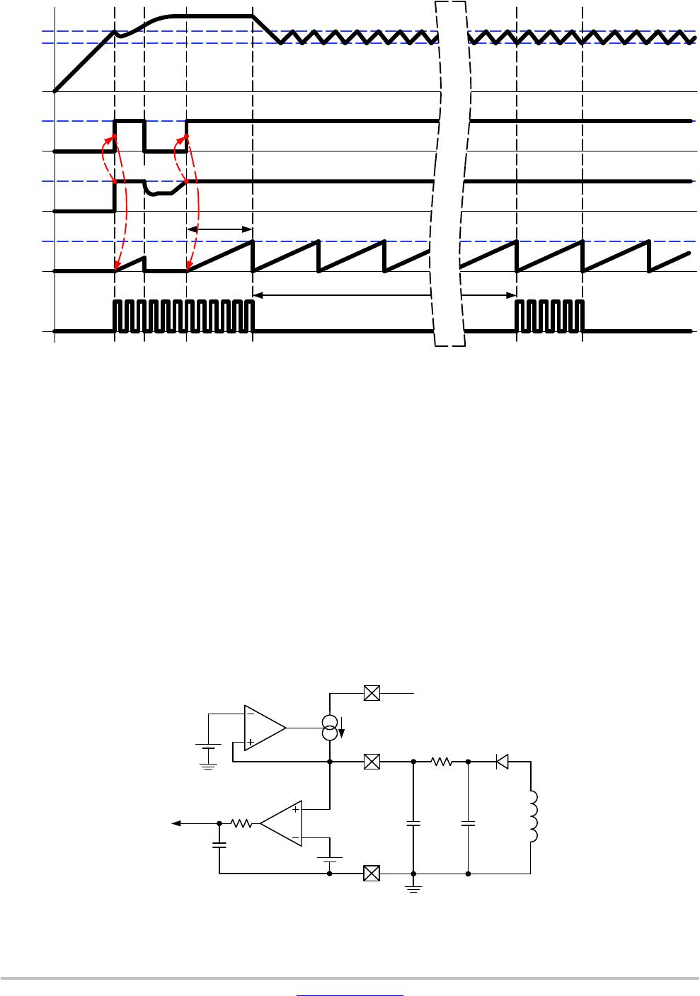
Fault Condition – Output Short−circuit
As soon as V
CC
reaches V
CC(ON)
, drive pulses are
internally enabled. If everything is correct, the auxiliary
winding increases the voltage on the VCC pin as the output
voltage rises. During the start−sequence, the controller
smoothly ramps up the peak drain current to maximum
setting, i.e. I
PK
, which is reached after a typical period of
10 ms. When the output voltage is not regulated, the current
coming through FB pin is below I
FBfault
level (35 mA
typically), which is not only during the start−up period but
also anytime an overload occurs, an internal error flag is
asserted, I
pFlag
, indicating that the system has reached its
maximum current limit set−point. The assertion of this flag
triggers a fault counter t
SCP
(48 ms typically). If at counter
completion, I
pFlag
remains asserted, all driving pulses are
stopped and the part stays off in t
recovery
duration (about
420 ms). A new attempt to re−start occurs and will last
48 ms providing the fault is still present. If the fault still
affects the output, a safe burst mode is entered, affected by
a low duty−cycle operation (11%). When the fault
disappears, the power supply quickly resumes operation.
Figure 35 depicts this particular mode: