NCP1075A/B, NCP1076A/B, NCP1077A/B, NCP1079A/B
www.onsemi.com
25
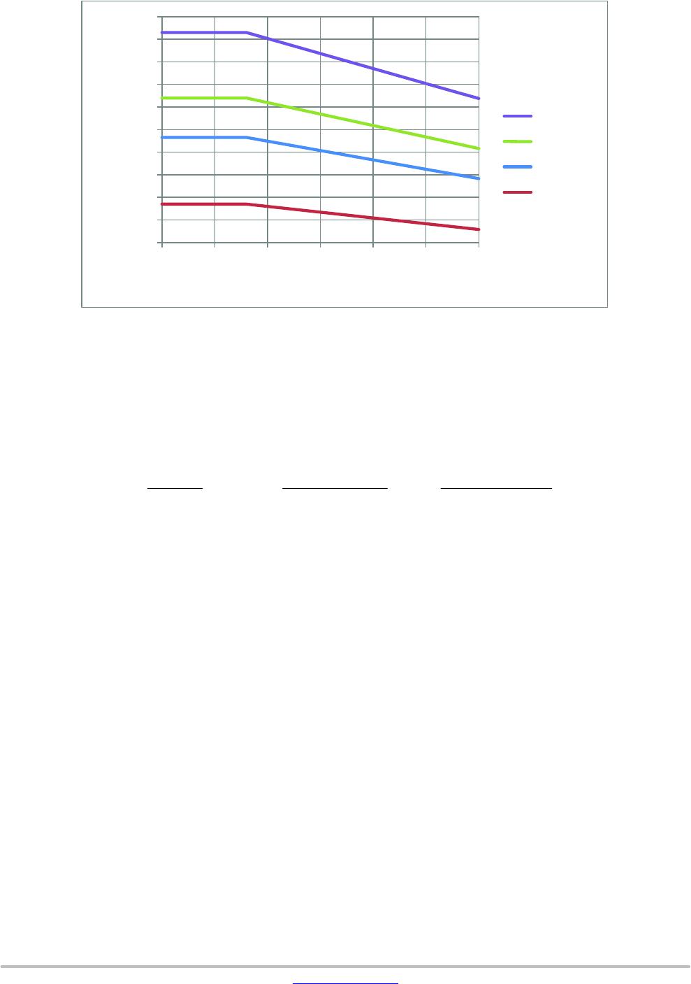
Figure 48. Current Set−point Dependence on BO/AC_OVP Pin Voltage
300
400
500
600
700
800
900
1000
1100
1200
1300
0 0.5 1.0 1.5 2.0 2.5 3.0
Max current set-point [mA]
V
BO/ACOVP
[V]
NCP1079u
NCP1077u
NCP1076u
NCP1075u
There are several known ways to implement Over−power
Protection (OPP), all suffering from particular problems.
These problems range from the added consumption burden
on the converter or the skip−cycle disturbance brought by
the current−sense offset. In this case is added consumption
due to resistive divider (Equation 2).
Maximum peak current is reduced internally according to
bulk voltage. When V
BO(OPP)
is maximum, the peak current
set−point is reduced by 10%. Bulk voltage at which will be
maximum current peak reduced by 20% (10% in
NCP1075u):
V
BULK(OPP)
+ V
BO(OPP)
@
V
BULK(ON)
V
BO(ON)
+ V
BO(OPP)
@
R
LOWER
) R
UPPER
R
LOWER
+ 2.65 @
100 @ 10
3
) 14 @ 10
6
100 @ 10
3
+ 375 Vdc + 265 Vrms
(eq. 5)
NCP1075A/B, NCP1076A/B, NCP1077A/B, NCP1079A/B
www.onsemi.com
26
Second LEB – Peak Current Protection
There is a second level of current protection with 100 ns
propagation delay to prevent IC against high peak current.
If peak current is 150% max peak current limit, then the
controller stops switching after three pulses and waits for an
auto−recovery period (t
recovery
) before attempting to
re−start.
Slope Compensation and I
PK
Set−point
In order to let the NCP107xu operate in CCM with a
duty−cycle above 50%, a fixed slope compensation is
internally applied to the current−mode control.
Below appears a table of the slope compensation level, the
initial current set−point, and the final current set−point of
different versions of switcher.
NCP1075u NCP1076u NCP1077u NCP1079u
f
SW
65 kHz 100 kHz 65 kHz 100 kHz 65 kHz 100 kHz 65 kHz 100 kHz
S
a
9 mA/ms 14 mA/ms 15 mA/ms 23 mA/ms 18 mA/ms 28 mA/ms 24 mA/ms 37 mA/ms
I
PK
(Duty−cycle = 50%) 400 mA 650 mA 800 mA 1050 mA
I
PK(0)
470 mA 765 mA 940 mA 1230 mA
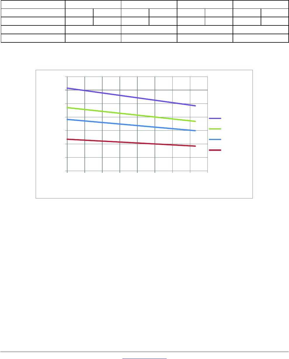
Figure 49 depicts the variation of I
PK
set−point vs. the power switcher duty ratio, which is caused by the internal ramp
compensation.
Figure 49. I
PK
Set−point varies with Power Switch On Time, which is Caused by the Ramp Compensation
0
200
400
600
800
1000
1200
1400
0 0.1 0.2 0.3 0.4 0.5 0.6 0.7 0.8
I
IPK
set-point [mA]
Duty Ratio [%]
NCP1079u
NCP1077u
NCP1076u
NCP1075u
NCP1075A/B, NCP1076A/B, NCP1077A/B, NCP1079A/B
www.onsemi.com
27
Design Procedure
The design of an SMPS around a monolithic device does
not differ from that of a standard circuit using a controller
and a MOSFET. However, one needs to be aware of certain
characteristics specific of monolithic devices. Let us follow
the steps:
V
IN,MIN
= 90 V rms or 127 V dc once rectified,
assuming a low bulk ripple
V
IN,MAX
= 265 V rms or 375 V dc
V
OUT
= 12 V
P
OUT
= 10 W
Operating mode is CCM
η = 0.8
1. The lateral MOSFET body−diode shall never be
forward biased, either during start−up (because of
a large leakage inductance) or in normal operation,
depicted by Figure 50. This condition sets the
maximum voltage that can be reflected during t
F
As a result, the flyback voltage which is reflected
on the drain at the switch opening cannot be larger
than the input voltage. When selecting
components, you thus must adopt a turn ratio
which adheres to the following equation:
N @
ǒ
V
OUT
) V
F
Ǔ
t V
IN,MIN
(eq. 6)
2. In our case, since we operate from a 127 V dc rail
while delivering 12 V, we can select a reflected
voltage of 120 V dc maximum. Therefore, the turn
ratio Np:Ns must be smaller than
V
reflect
V
OUT
) V
F
+
120
12 ) 0.5
+ 9.6orNp:Nst 9.6
Here we choose N = 8 in this case. We will see later
on how it affects the calculation.
Figure 50. The Drain−Source Wave Shall Always be Positive
I
PEAK
I
VALLEY
I
avg
I
Lavg
DT
sw
T
sw
I
L
t
D
I
L
Figure 51. Primary Inductance Current
Evolution in CCM
3. Lateral MOSFETs have a poorly doped
body−diode which naturally limits their ability to
sustain the avalanche. A traditional RCD clamping
network shall thus be installed to protect the
MOSFET. In some low power applications,
a simple capacitor can also be used since
V
DRAIN,MAX
+
(eq. 7)
V
IN
) N @
ǒ
V
OUT
) V
F
Ǔ
) I
PEAK
@
L
F
C
TOT
Ǹ
where L
F
is the leakage inductance, C
TOT
the total
capacitance at the drain node (which is increased by
the capacitor you will wire between drain and
source), N the N
P
:N
S
turn ratio, V
OUT
the output
voltage, V
F
the secondary diode forward drop and
finally,
I
PEAK
the maximum peak current. Worse
case occurs when the SMPS is very close to
regulation, e.g. the
V
OUT
target is almost reached
and
I
PEAK
is still pushed to the maximum. For this
NCP1075BAP130G

Mfr. #:
Manufacturer:
ON Semiconductor
Description:
AC/DC Converters ENHANCED OFF-LINE SWITCHE
Lifecycle:
New from this manufacturer.
Delivery:
DHL FedEx Ups TNT EMS
Payment:
T/T Paypal Visa MoneyGram Western Union