NCP1075A/B, NCP1076A/B, NCP1077A/B, NCP1079A/B
www.onsemi.com
22
V
BO(OFF)
V
BO(ON)
V
CC
V
B
O/AC_OVP
Drain
current
V
CC(MIN)
V
CC(ON)
Timer
50 ms
Soft−start Soft−start
Figure 43. Brown−out Functionality in Soft−start
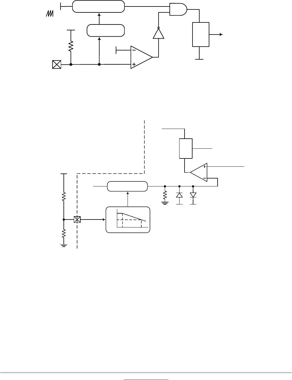
If voltage on VCC pin is higher than V
CC(ON)
and voltage
on BO/AC_OVP pin is higher than V
BO(ON)
then IC starts
pulsing, drain current is increasing for 10 ms (Soft−start).
Brown−out is inhibited during Soft−start, when Soft−start
ended, Brown−out checked if is voltage on BO/AC_OVP
pin higher than V
BO(OFF)
. If the voltage is lower, timer count
50 ms and if the voltage don’t increase over V
BO(OFF)
then
IC stops switching as one can see on Figure 43.
Frequency Foldback
The reduction of no−load standby power associated with
the need for improving the efficiency, requires to change the
traditional fixed−frequency type of operation. This device
implements a switching frequency folback when the
feedback current passes above a certain level, I
FBfold
, set
around 68 mA. At this point, the oscillator enters frequency
foldback and reduces its switching frequency.
The internal peak current set−point is following the
feedback current information until its level reaches the
minimal freezing level point of I
freeze
. Below this value, the
peak current set−point is frozen to 30% of the I
PK(0)
. The
only way to further reduce the transmitted power is to
diminish the operating frequency down to f
MIN
(27 kHz
typically). This value is reached at a feedback current level
of I
FBfold(END)
(100 mA typically). Below this point, if the
output power continues to decrease, the part enters skip
cycle for the best noise−free performance in no−load
conditions. Figures 44 and 45 depict the adopted scheme for
the part.
NCP1075A/B, NCP1076A/B, NCP1077A/B, NCP1079A/B
www.onsemi.com
23
Figure 44. By Observing the Current on the FB pin, the Controller Reduces its
Switching Frequency for an Improved Performance at Light Load
0
20
40
60
80
100
120
50 60 70 80 90 100
Frequency [kHz]
I
FB
[mA]
100 kHz
65 kHz
Figure 45. I
PK
Set−point is Frozen at Lower Power Demand
0
200
400
600
800
1000
1200
1400
40 50 60 70 80 90 100 110
Current set point [mA]
I
FB
[mA]
NCP1079u
NCP1077u
NCP1076u
NCP1075u
Feedback and Skip
The FB pin operates linearly as the absolute value of
feedback current (I
FB
) is above 40 mA. In this linear
operating range, the dynamic resistance is 19.5 kW typically
(R
FB(UP)
) and the effective pull up voltage is 3.3 V typically
(V
FB(REF)
). When I
FB
is decreased, the FB voltage will
increase to 3.3 V.
NCP1075A/B, NCP1076A/B, NCP1077A/B, NCP1079A/B
www.onsemi.com
24
Figure 46 depicts the skip mode block diagram. When the
FB current information reaches I
FB(skip)
, the internal clock
to set the flip−flop is blanked and the internal consumption
of the controller is decreased. The hysteresis of internal skip
comparator is minimized to lower the ripple of the auxiliary
voltage for VCC pin and V
OUT
of power supply during skip
mode. It easies the design of V
CC
overload range.
OSC
Jittering
Foldback
I
FB(skip )
R
FB (UP )
V
FB(REF )
S
R
Q
CS comparator
FB
SKIP
DRV stage
Figure 46. Skip Cycle Schematic
Over−power Protection
This function lets you limit the maximum dc output current regardless of the operating input voltage. For a correct operation,
the BO/AC_OVP pin must be connected via a resistive divider to observe the bulk voltage.
S
R
Q
I
FB
to CS setpoint
I
freeze
I
PK(0)
Vramp + Vsense
OSC
I
FB
MOSFET
R
UPPER
R
LOWER
V
BULK
BO/AC_OVP
2.65 V
V
BO (ON )
I
PK (0)
I
PK (OPP )
Figure 47. The OPP Circuity Affects the Maximum Peak
Current Set−point in Relationship to the Input Voltage.

NCP1075BAP130G

Mfr. #:
Manufacturer:
ON Semiconductor
Description:
AC/DC Converters ENHANCED OFF-LINE SWITCHE
Lifecycle:
New from this manufacturer.
Delivery:
DHL FedEx Ups TNT EMS
Payment:
T/T Paypal Visa MoneyGram Western Union