IDT8L3010I Data Sheet CRYSTAL OR DIFFERNTIALTO LVCMOS/LVTTL CLOCK BUFFER
IDT8L3010ANLGI REVISION A JANUARY 12, 2012 4 ©2012 Integrated Device Technology, Inc.
Absolute Maximum Ratings
NOTE: Stresses beyond those listed under Absolute Maximum Ratings may cause permanent damage to the device.
These ratings are stress specifications only. Functional operation of product at these conditions or any conditions beyond
those listed in the DC Characteristics or AC Characteristics is not implied. Exposure to absolute maximum rating conditions for
extended periods may affect product reliability.
DC Electrical Characteristics
Table 4A. Power Supply DC Characteristics, V
DD
= 3.3V±5%, V
DDO
= 3.3V±5% or 2.5V±5% or 1.8V±0.2V or 1.5V±0.15V,
T
A
= -40°C to 85°C
Item Rating
Supply Voltage, V
DD
3.63V
Inputs, V
I
CLK
X,
nCLK
X,
XTAL_IN
Other Inputs
0V to 5V
0V to 2V
-0.5V to V
DD
+ 0.5V
Outputs, V
O
-0.5V to V
DDO
+ 0.5V
Package Thermal Impedance,
JA
33.1°C/W (0 mps)
Storage Temperature, T
STG
-65C to 150C
Symbol Parameter Test Conditions Minimum Typical Maximum Units
V
DD
Power Supply Voltage 3.135 3.3 3.465 V
V
DDO
Output Supply Voltage
3.135 3.3 3.465 V
2.375 2.5 2.625 V
1.6 1.8 2 V
1.35 1.5 1.65 V
I
DD
Power Supply Current OE = 0 38 mA
I
DDO
Output Supply Current
OE = 1, V
DDO
= 3.3V±5%, Outputs Unloaded 5 mA
OE = 1, V
DDO
= 2.5V±5%, Outputs Unloaded 5 mA
OE = 1, V
DDO
= 1.8V±0.2V, Outputs Unloaded 5 mA
OE = 1, V
DDO
= 1.5V±0.15V, Outputs Unloaded 5 mA
IDT8L3010I Data Sheet CRYSTAL OR DIFFERNTIALTO LVCMOS/LVTTL CLOCK BUFFER
IDT8L3010ANLGI REVISION A JANUARY 12, 2012 5 ©2012 Integrated Device Technology, Inc.
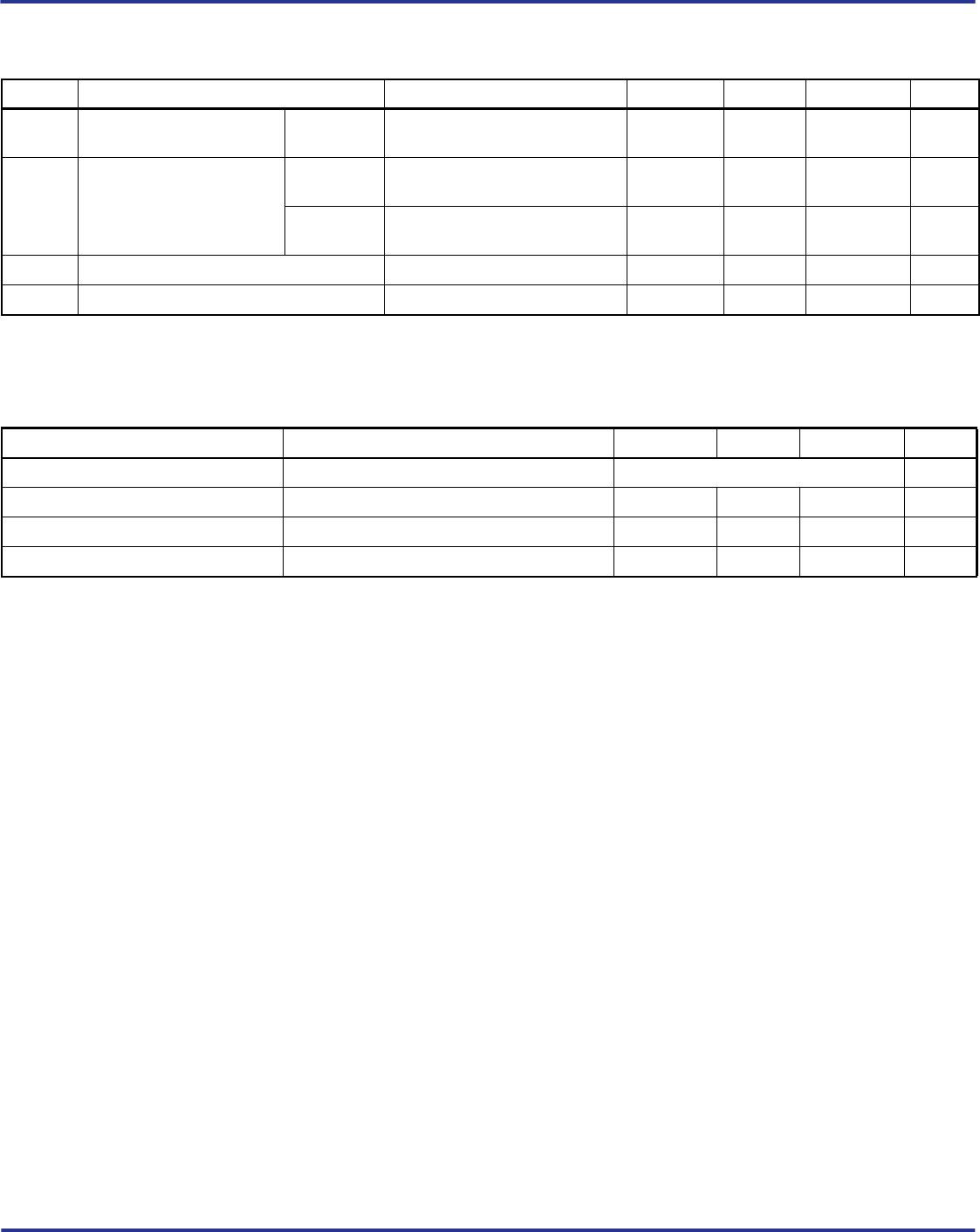
Table 4B. Power Supply DC Characteristics, V
DD
= 2.5V±5%, V
DDO
= 2.5V±5% or 1.8V±0.2V or 1.5V±0.15V,
T
A
= -40°C to 85°C
Table 4C. LVCMOS/LVTTL DC Characteristics, T
A
= -40°C to 85°C
NOTE 1: Outputs terminated with 50 to V
DDO
/2. See Parameter Measurement Information, Output Load Test Circuit diagrams.
Symbol Parameter Test Conditions Minimum Typical Maximum Units
V
DD
Power Supply Voltage 2.375 2.5 2.625 V
V
DDO
Output Supply Current
2.375 2.5 2.625 V
1.6 1.8 2 V
1.35 1.5 1.65 V
I
DD
Power Supply Current OE = 0 38 mA
I
DDO
Output Supply Current
OE = 1, V
DDO
= 2.5V±5%, Outputs Unloaded 5 mA
OE = 1, V
DDO
= 1.8V±0.2V, Outputs Unloaded 5 mA
OE = 1, V
DDO
= 1.5V±0.15V, Outputs Unloaded 5 mA
Symbol Parameter Test Conditions Minimum Typical Maximum Units
V
IH
Input High Voltage
V
DD
= 3.3V±5% 2 V
DD
+ 0.3 V
V
DD
= 2.5V±5% 1.7 V
DD
+ 0.3 V
V
IL
Input Low Voltage
V
DD
= 3.3V±5% -0.3 0.8 V
V
DD
= 2.5V±5% -0.3 0.7 V
I
IH
Input High Current OE, SEL[1:0] V
DD
= V
IN
= 3.465V 150 µA
I
IL
Input Low Current OE, SEL[1:0] V
DD
= 3.465V, V
IN
= 0V -5 µA
V
OH
Output High Voltage; NOTE 1
V
DDO
= 3.3V±5% 2.6 V
V
DDO
= 2.5V±5% 1.8 V
V
DDO
= 1.8V±0.2V 1.2 V
V
DDO
= 1.5V±0.15V 0.97 V
V
OL
Output Low Voltage; NOTE 1
V
DDO
= 3.3V±5% or 2.5V±5% 0.5 V
V
DDO
= 1.8V±0.2V 0.4 V
V
DDO
= 1.5V±0.15V 0.37 V
IDT8L3010I Data Sheet CRYSTAL OR DIFFERNTIALTO LVCMOS/LVTTL CLOCK BUFFER
IDT8L3010ANLGI REVISION A JANUARY 12, 2012 6 ©2012 Integrated Device Technology, Inc.
Table 4D. Differential DC Characteristics, V
DD
= 3.3V±5% or 2.5V±5%, T
A
= -40°C to 85°C
NOTE 1: V
IL
should not be less than -0.3V.
NOTE 2. Common mode voltage is defined at the crosspoint.
Table 5. Crystal Characteristics
NOTE: Characterized using a 12pF parallel resonant crystal.
Symbol Parameter Test Conditions Minimum Typical Maximum Units
I
IH
Input High Current
CLK[0:1],
nCLK[0:1]
V
DD
= V
IN
= 3.465V or 2.625V 150 µA
I
IL
Input Low Current
CLK[0:1]
V
DD
= 3.465V or 2.625V,
V
IN
= 0V
-5 µA
nCLK[0:1]
V
DD
= 3.465V or 2.625V,
V
IN
= 0V
-150 µA
V
PP
Peak-to-Peak Input Voltage; NOTE 1 0.15 1.3 V
V
CMR
Common Mode Input Voltage; NOTE 1, 2 0.5 V
DD
– 0.85 V
Parameter Test Conditions Minimum Typical Maximum Units
Mode of Oscillation Fundamental
Frequency 10 40 MHz
Equivalent Series Resistance (ESR) 50
Shunt Capacitance 7pF

8L3010ANLGI

Mfr. #:
Manufacturer:
IDT
Description:
Clock Buffer Crystal Or Differential to LVCMOS/LVTTL Clock Buffer
Lifecycle:
New from this manufacturer.
Delivery:
DHL FedEx Ups TNT EMS
Payment:
T/T Paypal Visa MoneyGram Western Union

Products related to this Datasheet