IDT8L3010I Data Sheet CRYSTAL OR DIFFERNTIALTO LVCMOS/LVTTL CLOCK BUFFER
IDT8L3010ANLGI REVISION A JANUARY 12, 2012 7 ©2012 Integrated Device Technology, Inc.
AC Electrical Characteristics
Table 6. AC Characteristics, V
DD
= 3.3V±5%, V
DDO
= 3.3V±5% or 2.5V±5% or 1.8V±0.2V or 1.5V±0.15V,
T
A
= -40°C to 85°C
NOTE: Electrical parameters are guaranteed over the specified ambient operating temperature range, which is established when the device
is mounted in a test socket with maintained transverse airflow greater than 500 lfpm. The device will meet specifications after thermal
equilibrium has been reached under these conditions.
All parameters measured at ƒ f
OUT
unless noted otherwise.
NOTE 1: Defined as skew between outputs at the same supply voltage and with equal load conditions. Measured at V
DDO
/2.
NOTE 2: This parameter is defined in accordance with JEDEC Standard 65.
NOTE 3: These parameters are guaranteed by characterization. Not tested in production.
Symbol Parameter Test Conditions Minimum Typical Maximum Units
f
OUT
Output Frequency
Using External Crystal 10 40 MHz
Using External Clock
Source
200 MHz
tsk(o) Output Skew; NOTE 1, 2
V
DDO
= 3.3V ± 5% 10 50 ps
V
DDO
= 2.5V ± 5% 10 50 ps
V
DDO
= 1.8V ± 0.2V 10 55 ps
V
DDO
= 1.5V ± 0.15V 15 75 ps
tjit
Buffer Additive
Phase Jitter; refer to
Additive Phase Jitter
Section; NOTE 3,
f
OUT
= 125MHz,
Integration Range:
12kHz - 20MHz
Input Clock from
CLK0, nCLK0 or
CLK1, nCLK1
V
DDO
= 3.3V ± 5% 0.24 0.35 ps
V
DDO
= 2.5V ± 5% 0.29 0.39 ps
V
DDO
= 1.8V ± 0.2V 0.32 0.43 ps
V
DDO
= 1.5V ± 0.15V 0.37 0.66 ps
tjit(Ø)
RMS Phase Jitter;
NOTE 3,
Integration Range:
12kHz - 5MHz
Input Clock from
25MHz Crystal
V
DDO
= 3.3V ± 5% 0.20 0.27 ps
V
DDO
= 2.5V ± 5% 0.23 0.29 ps
V
DDO
= 1.8V ± 0.2V 0.26 0.37 ps
V
DDO
= 1.5V ± 0.15V 0.33 0.63 ps
t
R
/ t
F
Output
Rise/Fall Time
V
DDO
= 3.3V ± 5% 20% to 80% 150 450 ps
V
DDO
= 2.5V ± 5% 20% to 80% 200 500 ps
V
DDO
= 1.8V ± 0.2V 20% to 80% 200 800 ps
V
DDO
= 1.5V ± 0.15V 20% to 80% 250 1000 ps
odc Output Duty Cycle
V
DDO
= 3.3V ± 5% f
OUT
156.25MHz 44 56 %
V
DDO
= 2.5V ± 5% 40 60 %
V
DDO
= 1.8V ± 0.2V 40 60 %
V
DDO
= 1.5V ± 0.15V 40 60 %
MUX_
ISOLATION
MUX Isolation; NOTE 3 155.52MHz 65 dB
IDT8L3010I Data Sheet CRYSTAL OR DIFFERNTIALTO LVCMOS/LVTTL CLOCK BUFFER
IDT8L3010ANLGI REVISION A JANUARY 12, 2012 8 ©2012 Integrated Device Technology, Inc.
Typical Phase Noise at 25MHz (3.3V)
Noise Power dBc
Hz
Offset Frequency (Hz)
IDT8L3010I Data Sheet CRYSTAL OR DIFFERNTIALTO LVCMOS/LVTTL CLOCK BUFFER
IDT8L3010ANLGI REVISION A JANUARY 12, 2012 9 ©2012 Integrated Device Technology, Inc.
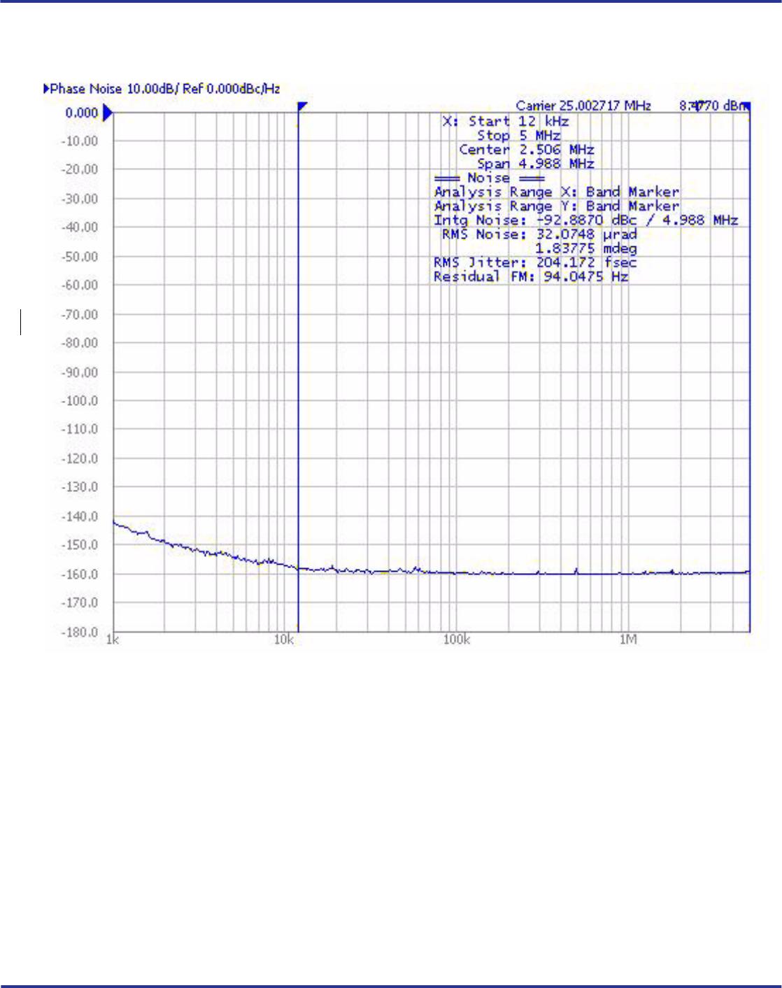
Additive Phase Jitter (3.3V)
The spectral purity in a band at a specific offset from the fundamental
compared to the power of the fundamental is called the dBc Phase
Noise. This value is normally expressed using a Phase noise plot
and is most often the specified plot in many applications. Phase noise
is defined as the ratio of the noise power present in a 1Hz band at a
specified offset from the fundamental frequency to the power value of
the fundamental. This ratio is expressed in decibels (dBm) or a ratio
of the power in the 1Hz band to the power in the fundamental. When
the required offset is specified, the phase noise is called a dBc value,
which simply means dBm at a specified offset from the fundamental.
By investigating jitter in the frequency domain, we get a better
understanding of its effects on the desired application over the entire
time record of the signal. It is mathematically possible to calculate an
expected bit error rate given a phase noise plot.
As with most timing specifications, phase noise measurements has
issues relating to the limitations of the equipment. Often the noise
floor of the equipment is higher than the noise floor of the device. The
phase noise is dependent on the input source and measurement
equipment.
The signal generator used is, “Rohde & Schwarz SMA100A,
measured with Agilent 5052A”.
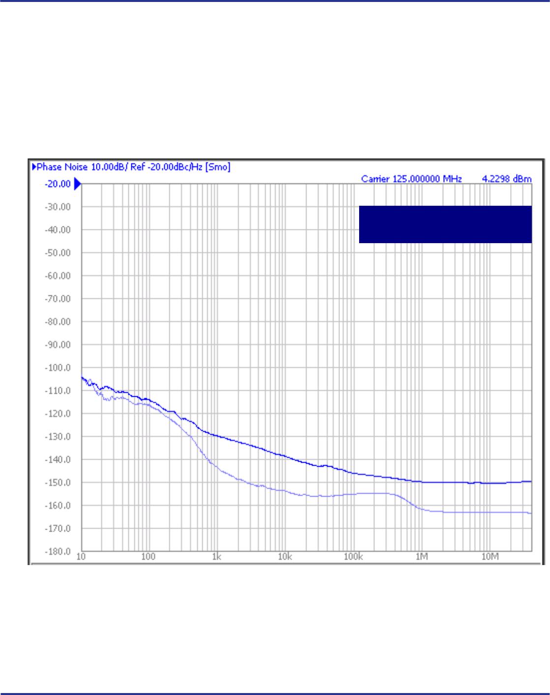
8L3010ANLGI

Mfr. #:
Manufacturer:
IDT
Description:
Clock Buffer Crystal Or Differential to LVCMOS/LVTTL Clock Buffer
Lifecycle:
New from this manufacturer.
Delivery:
DHL FedEx Ups TNT EMS
Payment:
T/T Paypal Visa MoneyGram Western Union

Products related to this Datasheet