74LVC161 All information provided in this document is subject to legal disclaimers. © NXP B.V. 2013. All rights reserved.
Product data sheet Rev. 6 — 30 September 2013 9 of 22
NXP Semiconductors
74LVC161
Presettable synchronous 4-bit binary counter; asynchronous reset
[1] All typical values are measured at V
CC
= 3.3 V (unless stated otherwise) and T
amb
=25C.
10. Dynamic characteristics
I
CC
supply
current
V
CC
= 3.6 V; V
I
=V
CC
or GND;
I
O
=0A
-0.110-40A
I
CC
additional
supply
current
per input pin;
V
CC
= 2.7 V to 3.6 V;
V
I
=V
CC
0.6 V; I
O
=0A
- 5 500 - 5000 A
C
I
input
capacitance
V
CC
= 0 V to 3.6 V;
V
I
=GNDtoV
CC
-5.0---pF
Table 6. Static characteristics
…continued
At recommended operating conditions. Voltages are referenced to GND (ground = 0 V).
Symbol Parameter Conditions 40 C to +85 C 40 C to +125 C Unit
Min Typ
[1]
Max Min Max
Table 7. Dynamic characteristics
Voltages are referenced to GND (ground = 0 V). For test circuit see Figure 14
.
Symbol Parameter Conditions 40 C to +85 C 40 C to +125 C Unit
Min Typ
[1]
Max Min Max
t
pd
propagation
delay
CP to Qn; see Figure 9
[2]
V
CC
= 1.2 V - 17 - - - ns
V
CC
= 1.65 V to 1.95 V 1.5 7.0 14.5 1.5 16.7 ns
V
CC
= 2.3 V to 2.7 V 2.5 4.0 8.1 2.5 9.4 ns
V
CC
= 2.7 V 1.5 3.8 7.2 1.5 9.0 ns
V
CC
= 3.0 V to 3.6 V 1.5 3.6 7.3 1.5 9.5 ns
CP to TC; see Figure 9
[2]
V
CC
= 1.2 V - 20 - - - ns
V
CC
= 1.65 V to 1.95 V 1.8 8.1 15.5 1.8 17.9 ns
V
CC
= 2.3 V to 2.7 V 2.8 4.6 8.7 2.8 10.1 ns
V
CC
= 2.7 V 1.5 4.3 7.8 1.5 10.0 ns
V
CC
= 3.0 V to 3.6 V 1.5 4.2 7.8 1.5 10.0 ns
CET to TC; see Figure 10
[2]
V
CC
= 1.2 V - 16 - - - ns
V
CC
= 1.65 V to 1.95 V 1.5 5.9 11.9 1.5 13.7 ns
V
CC
= 2.3 V to 2.7 V 1.9 3.4 6.7 1.9 7.7 ns
V
CC
= 2.7 V 1.5 3.6 6.5 1.5 8.5 ns
V
CC
= 3.0 V to 3.6 V 1.5 3.1 6.0 1.5 7.5 ns
74LVC161 All information provided in this document is subject to legal disclaimers. © NXP B.V. 2013. All rights reserved.
Product data sheet Rev. 6 — 30 September 2013 10 of 22
NXP Semiconductors
74LVC161
Presettable synchronous 4-bit binary counter; asynchronous reset
t
PHL
HIGH to LOW
propagation
delay
MR to Qn; see Figure 11
V
CC
= 1.2 V - 17 - - - ns
V
CC
= 1.65 V to 1.95 V 1.5 6.2 12.7 1.5 14.6 ns
V
CC
= 2.3 V to 2.7 V 1.9 3.6 7.1 1.9 8.3 ns
V
CC
= 2.7 V 1.5 3.9 7.1 1.5 9.0 ns
V
CC
= 3.0 V to 3.6 V 1.5 3.2 6.4 1.5 8.0 ns
MR
to TC; see Figure 11
V
CC
= 1.2 V - 18 - - - ns
V
CC
= 1.65 V to 1.95 V 1.7 8.3 15.9 1.7 18.4 ns
V
CC
= 2.3 V to 2.7 V 2.7 4.8 8.9 2.7 10.3 ns
V
CC
= 2.7 V 1.5 4.9 8.6 1.5 11.0 ns
V
CC
= 3.0 V to 3.6 V 1.5 4.3 8.0 1.5 10.0 ns
t
W
pulse width clock HIGH or LOW; see Figure 9
V
CC
= 1.65 V to 1.95 V 6.0 - - 6.0 - ns
V
CC
= 2.3 V to 2.7 V 5.0 - - 5.0 - ns
V
CC
= 2.7 V 5.0 - - 5.0 - ns
V
CC
= 3.0 V to 3.6 V 4.0 1.2 - 4.0 - ns
master reset LOW; see Figure 11
V
CC
= 1.65 V to 1.95 V 5.0 - - 5.0 - ns
V
CC
= 2.3 V to 2.7 V 4.0 - - 4.0 - ns
V
CC
= 2.7 V 4.0 - - 4.0 - ns
V
CC
= 3.0 V to 3.6 V 3.0 1.6 - 3.0 - ns
t
rec
recovery time MR to CP; see Figure 11
V
CC
= 1.65 V to 1.95 V 1.0 - - 1.0 - ns
V
CC
= 2.3 V to 2.7 V 1.0 - - 1.0 - ns
V
CC
= 2.7 V 0.0 - - 0.0 - ns
V
CC
= 3.0 V to 3.6 V 0.5 0.0 - 0.5 - ns
Table 7. Dynamic characteristics
…continued
Voltages are referenced to GND (ground = 0 V). For test circuit see Figure 14.
Symbol Parameter Conditions 40 C to +85 C 40 C to +125 C Unit
Min Typ
[1]
Max Min Max
74LVC161 All information provided in this document is subject to legal disclaimers. © NXP B.V. 2013. All rights reserved.
Product data sheet Rev. 6 — 30 September 2013 11 of 22
NXP Semiconductors
74LVC161
Presettable synchronous 4-bit binary counter; asynchronous reset
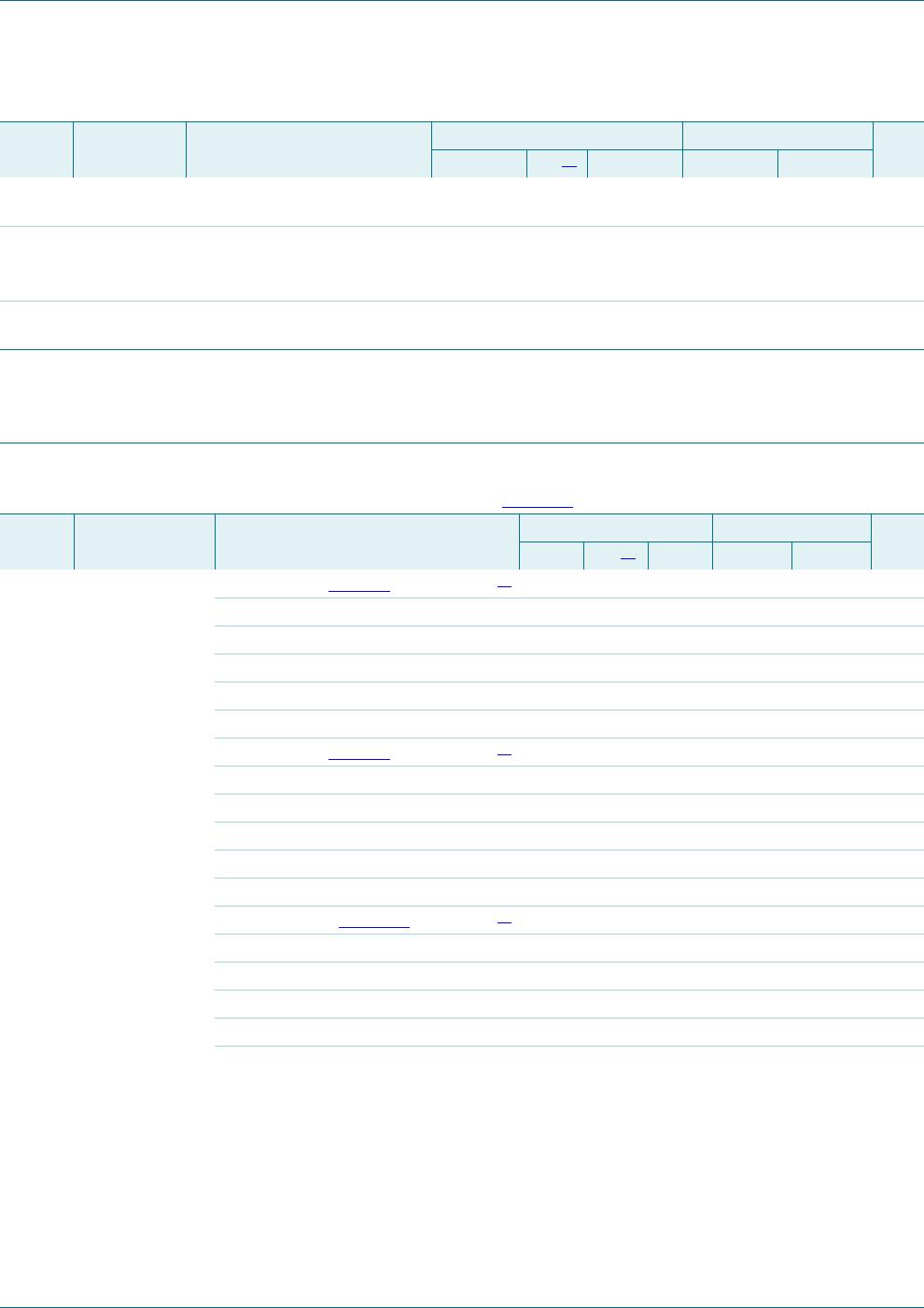
[1] Typical values are measured at T
amb
=25C and V
CC
= 1.2 V, 1.8 V, 2.5 V, 2.7 V and 3.3 V respectively.
[2] t
pd
is the same as t
PLH
and t
PHL
.
[3] Skew between any two outputs of the same package switching in the same direction. This parameter is guaranteed by design.
[4] C
PD
is used to determine the dynamic power dissipation (P
D
in W).
P
D
=C
PD
V
CC
2
f
i
N+(C
L
V
CC
2
f
o
) where:
f
i
= input frequency in MHz; f
o
= output frequency in MHz
C
L
= output load capacitance in pF
V
CC
= supply voltage in V
N = number of inputs switching
(C
L
V
CC
2
f
o
) = sum of outputs
t
su
set-up time Dn to CP; see Figure 12
V
CC
= 1.65 V to 1.95 V 5.0 - - 5.0 - ns
V
CC
= 2.3 V to 2.7 V 4.0 - - 4.0 - ns
V
CC
= 2.7 V 3.0 - - 3.0 - ns
V
CC
= 3.0 V to 3.6 V 2.5 1.0 - 2.5 - ns
PE
to CP; see Figure 12
V
CC
= 1.65 V to 1.95 V 4.5 - - 4.5 - ns
V
CC
= 2.3 V to 2.7 V 4.0 - - 4.0 - ns
V
CC
= 2.7 V 3.5 - - 3.5 - ns
V
CC
= 3.0 V to 3.6 V 3.0 1.2 - 3.0 - ns
CEP, CET to CP; see Figure 13
V
CC
= 1.65 V to 1.95 V 8.0 - - 8.0 - ns
V
CC
= 2.3 V to 2.7 V 6.0 - - 6.0 - ns
V
CC
= 2.7 V 5.5 - - 5.5 - ns
V
CC
= 3.0 V to 3.6 V 5.0 2.1 - 5.0 - ns
t
h
hold time Dn, PE, CEP, CET to CP; see
Figure 12 and 13
V
CC
= 1.65 V to 1.95 V 3.0 - - 3.0 - ns
V
CC
= 2.3 V to 2.7 V 2.5 - - 2.5 - ns
V
CC
= 2.7 V 0.0 - - 0.0 - ns
V
CC
= 3.0 V to 3.6 V 0.5 0.0 - 0.5 - ns
f
max
maximum
frequency
see Figure 9
V
CC
= 1.65 V to 1.95 V 100 - - 80 - MHZ
V
CC
= 2.3 V to 2.7 V 125 - - 100 - MHZ
V
CC
= 2.7 V 150 - - 120 - MHz
V
CC
= 3.0 V to 3.6 V 150 200 - 120 - MHz
t
sk(o)
output skew time V
CC
= 3.0 V to 3.6 V
[3]
- - 1.0 - 1.5 ns
C
PD
power dissipation
capacitance
per input; V
I
= GND to V
CC
[4]
V
CC
= 1.65 V to 1.95 V - 11.1 - pF
V
CC
= 2.3 V to 2.7 V - 14.7 - pF
V
CC
= 3.0 V to 3.6 V - 17.9 - pF
Table 7. Dynamic characteristics …continued
Voltages are referenced to GND (ground = 0 V). For test circuit see Figure 14.
Symbol Parameter Conditions 40 C to +85 C 40 C to +125 C Unit
Min Typ
[1]
Max Min Max

74LVC161D,118

Mfr. #:
Manufacturer:
Nexperia
Description:
Counter ICs 3.3V SYNC 4-BIT BIN
Lifecycle:
New from this manufacturer.
Delivery:
DHL FedEx Ups TNT EMS
Payment:
T/T Paypal Visa MoneyGram Western Union