74LVC161 All information provided in this document is subject to legal disclaimers. © NXP B.V. 2013. All rights reserved.
Product data sheet Rev. 6 — 30 September 2013 12 of 22
NXP Semiconductors
74LVC161
Presettable synchronous 4-bit binary counter; asynchronous reset
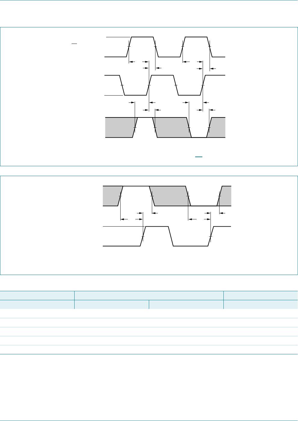
11. Waveforms
Measurement points are given in Table 8.
V
OL
and V
OH
are typical output voltage levels that occur with the output load.
Fig 9. Clock (CP) to outputs (Qn, TC) propagation delays, the clock pulse width, and maximum frequency
mna911
CP
input
Qn, TC
output
t
PHL
t
PLH
t
W
1/f
max
V
M
V
OH
V
I
GND
V
OL
V
M
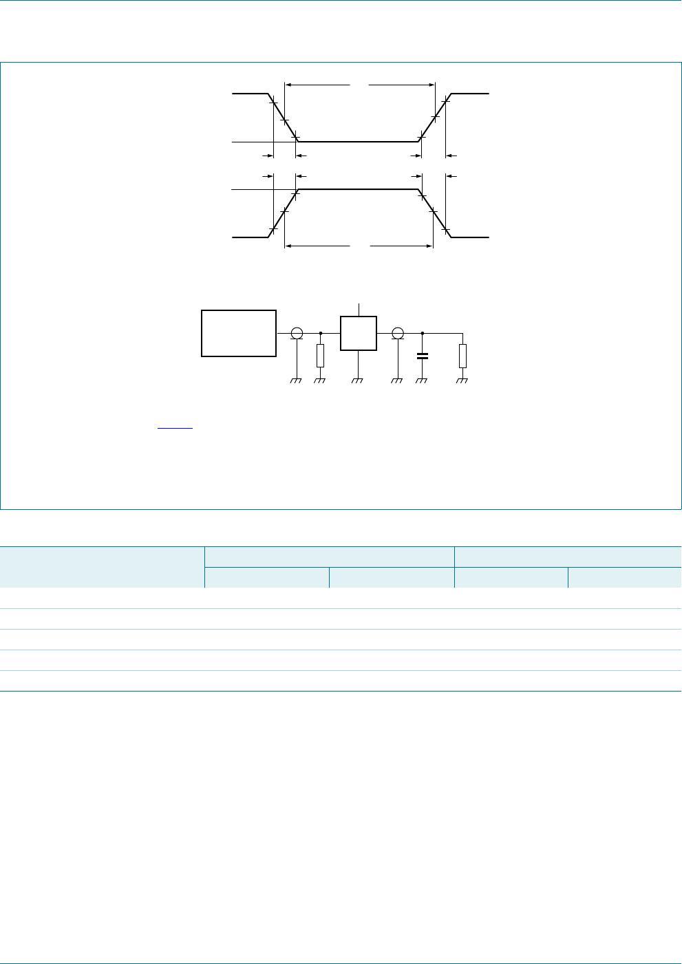
Measurement points are given in Table 8.
V
OL
and V
OH
are typical output voltage levels that occur with the output load.
Fig 10. Input (CET) to output (TC) propagation delays
mna912
t
PHL
t
PLH
V
M
V
M
TC output
CET input
GND
V
I
V
OH
V
OL
Fig 11. Master reset (MR) pulse width, the master reset to output (Qn, TC) propagation delays, and the master
reset to clock (CP) removal times
mna913
MR
input
CP
input
Qn, TC output
t
PHL
t
W
t
rec
V
M
V
OH
V
I
V
I
GND
GND
V
OL
V
M
V
M