74LVC161 All information provided in this document is subject to legal disclaimers. © NXP B.V. 2013. All rights reserved.
Product data sheet Rev. 6 — 30 September 2013 6 of 22
NXP Semiconductors
74LVC161
Presettable synchronous 4-bit binary counter; asynchronous reset
Fig 8. Logic diagram
PQD
4
7&
4
4
4
'
))
4
&
3
3
(
&(
3
&(
7
'
' ' '
&3
0
5
'
))
4
&3
'
))
4
&3
'
))
5
'
5
'
5
'
5
'
4
&3
4 4 4 4
74LVC161 All information provided in this document is subject to legal disclaimers. © NXP B.V. 2013. All rights reserved.
Product data sheet Rev. 6 — 30 September 2013 7 of 22
NXP Semiconductors
74LVC161
Presettable synchronous 4-bit binary counter; asynchronous reset
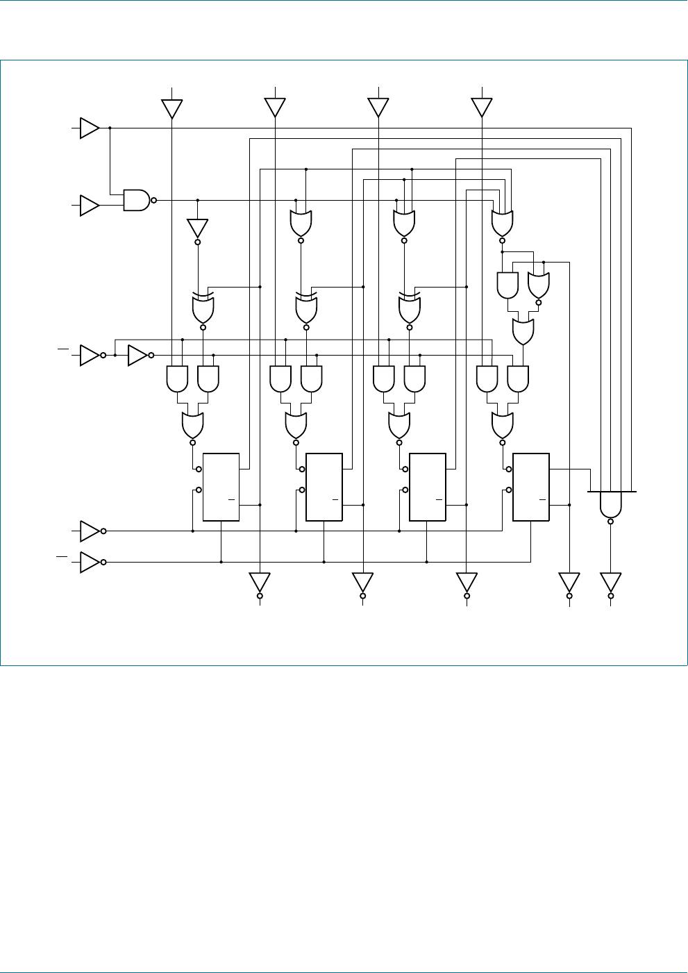
6. Functional description
[1] * = the TC output is HIGH when CET is HIGH and the counter is at terminal count (HHHH)
H = HIGH voltage level
h = HIGH voltage level one set-up time prior to the LOW-to-HIGH clock transition
L = LOW voltage level
l = LOW voltage level one set-up time prior to the LOW-to-HIGH clock transition
q = lower case letters indicate the state of the referenced output one set-up time prior to the LOW-to-HIGH clock transition
X = don’t care
= LOW-to-HIGH clock transition
7. Limiting values
[1] The minimum input voltage ratings may be exceeded if the input current ratings are observed.
[2] The output voltage ratings may be exceeded if the output current ratings are observed.
[3] For SO16 packages: above 70 C the value of P
D
derates linearly with 8 mW/K.
For (T)SSOP16 packages: above 60 C the value of P
D
derates linearly with 5.5 mW/K.
For DHVQFN16 packages: above 60 C the value of P
D
derates linearly with 4.5 mW/K.
Table 3. Function table
[1]
Operating
modes
Input Output
MR CP CEP CET PE Dn Qn TC
Reset (clear)LXXXXXLL
Parallel load H XXl l LL
H XXl hH*
Count H hhhXcount*
Hold
(do nothing)
HX l X h X q
n
*
HX X l h X q
n
L
Table 4. Limiting values
In accordance with the Absolute Maximum Rating System (IEC 60134). Voltages are referenced to GND (ground = 0 V).
Symbol Parameter Conditions Min Max Unit
V
CC
supply voltage 0.5 +6.5 V
I
IK
input clamping current V
I
<0 50 - mA
V
I
input voltage
[1]
0.5 +6.5 V
I
OK
output clamping current V
O
>V
CC
or V
O
<0 - 50 mA
V
O
output voltage
[2]
0.5 V
CC
+0.5 V
I
O
output current V
O
=0V toV
CC
- 50 mA
I
CC
supply current - 100 mA
I
GND
ground current 100 - mA
T
stg
storage temperature 65 +150 C
P
tot
total power dissipation T
amb
= 40 C to +125 C
[3]
-500mW
74LVC161 All information provided in this document is subject to legal disclaimers. © NXP B.V. 2013. All rights reserved.
Product data sheet Rev. 6 — 30 September 2013 8 of 22
NXP Semiconductors
74LVC161
Presettable synchronous 4-bit binary counter; asynchronous reset
8. Recommended operating conditions
9. Static characteristics
Table 5. Recommended operating conditions
Symbol Parameter Conditions Min Typ Max Unit
V
CC
supply voltage 1.65 - 3.6 V
functional 1.2 - - V
V
I
input voltage 0 - 5.5 V
V
O
output voltage 0 - V
CC
V
T
amb
ambient temperature in free air 40 - +125 C
t/V input transition rise and fall rate V
CC
= 1.65 V to 2.7 V 0 - 20 ns/V
V
CC
= 2.7 V to 3.6 V 0 - 10 ns/V
Table 6. Static characteristics
At recommended operating conditions. Voltages are referenced to GND (ground = 0 V).
Symbol Parameter Conditions 40 C to +85 C 40 C to +125 C Unit
Min Typ
[1]
Max Min Max
V
IH
HIGH-level
input voltage
V
CC
= 1.2 V 1.08 - - 1.08 - V
V
CC
= 1.65 V to 1.95 V 0.65 V
CC
- - 0.65 V
CC
-V
V
CC
= 2.3 V to 2.7 V 1.7 - - 1.7 - V
V
CC
= 2.7 V to 3.6 V 2.0 - - 2.0 - V
V
IL
LOW-level
input voltage
V
CC
= 1.2 V - - 0.12 - 0.12 V
V
CC
= 1.65 V to 1.95 V - - 0.35 V
CC
-0.35 V
CC
V
V
CC
= 2.3 V to 2.7 V - - 0.7 - 0.7 V
V
CC
= 2.7 V to 3.6 V - - 0.8 - 0.8 V
V
OH
HIGH-level
output
voltage
V
I
=V
IH
or V
IL
I
O
= 100 A;
V
CC
=1.65Vto3.6V
V
CC
0.2 - - V
CC
0.3 - V
I
O
= 4mA; V
CC
= 1.65 V 1.2 - - 1.05 - V
I
O
= 8mA; V
CC
= 2.3 V 1.8 - - 1.65 - V
I
O
= 12 mA; V
CC
= 2.7 V 2.2 - - 2.05 - V
I
O
= 18 mA; V
CC
= 3.0 V 2.4 - - 2.25 - V
I
O
= 24 mA; V
CC
= 3.0 V 2.2 - - 2.0 - V
V
OL
LOW-level
output
voltage
V
I
=V
IH
or V
IL
I
O
= 100 A;
V
CC
= 1.65 V to 3.6 V
- - 0.2 - 0.3 V
I
O
=4mA; V
CC
= 1.65 V - - 0.45 - 0.65 V
I
O
=8mA; V
CC
= 2.3 V - - 0.6 - 0.8 V
I
O
=12mA; V
CC
= 2.7 V - - 0.4 - 0.6 V
I
O
=24mA; V
CC
= 3.0 V - - 0.55 - 0.8 V
I
I
input leakage
current
V
CC
= 3.6 V; V
I
=5.5VorGND - 0.1 5- 20 A

74LVC161D,118

Mfr. #:
Manufacturer:
Nexperia
Description:
Counter ICs 3.3V SYNC 4-BIT BIN
Lifecycle:
New from this manufacturer.
Delivery:
DHL FedEx Ups TNT EMS
Payment:
T/T Paypal Visa MoneyGram Western Union