MC10EP142, MC100EP142
www.onsemi.com
10
Table 11. AC CHARACTERISTICS V
CC
= 3.0 V to 5.5 V; V
EE
= 0.0 V or V
CC
= 0.0 V; V
EE
= −3.0 V to −5.5 V (Note 26)
Symbol Unit
85°C25°C−40°C
Characteristic
Symbol Unit
MaxTypMinMaxTypMinMaxTypMin
Characteristic
t
h
Hold Time
D
SEL
100
50
50
−50
100
50
50
−50
100
50
50
−50
ps
t
RR
Reset Recovery Time 800 ps
t
pw
Minimum Pulse Width 200 ps
t
SKEW
Within-Device Skew (Note 27) Q, Q
Duty Cycle Skew (Note 28)
50
5.0
100
20
50
5.0
100
20
50
5.0
100
20
ps
t
JITTER
Random Clock Jitter (Figure 4) 1 2 1 2 1 2 ps
V
inpp
Input Voltage Swing/Sensitivity
(Differential Configuration)
150 800 1200 150 800 1200 150 800 1200 mV
t
r
,
t
f
Rise/Fall Times @ 50 MHz
(20 - 80%)
110 180 250 125 190 275 150 215 300 ps
NOTE: Device will meet the specifications after thermal equilibrium has been established when mounted in a test socket or printed circuit
board with maintained transverse airflow greater than 500 lfpm.
26.Measured using a 750 mV source, 50% duty cycle clock source. All loading with 50 W to V
CC
− 2.0 V.
27.Within-device skew is defined as identical transitions on similar paths through a device.
28.Skew is measured between outputs under identical transitions. Duty cycle skew is defined only for differential operation when the delays
are measured from the cross point of the inputs to the cross point of the outputs.
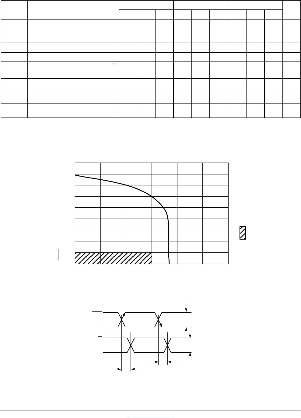
0
100
200
300
400
500
600
700
800
900
0 1000 2000 3000 4000 5000 6000
Figure 4. Output Voltage Amplitude / RMS Jitter vs.
Input Frequency at Ambient Temperature (Typical)
INPUT FREQUENCY (MHz)
1
2
3
4
5
6
7
8
9
Output Voltage Amplitude (mV)
JITTER
OUT
ps (RMS)
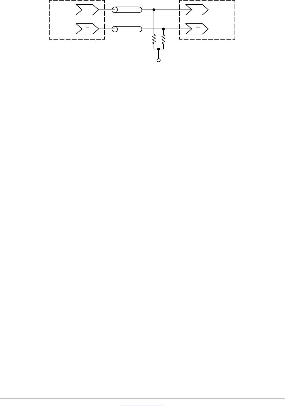
Figure 5. AC Reference Measurement
CLK
CLK
Q
Q
t
PHL
t
PLH
V
INPP
= V
IH
(CLK) − V
IL
(CLK)
V
OUTPP
= V
OH
(Q) − V
OL
(Q)