MC10EP142, MC100EP142
www.onsemi.com
7
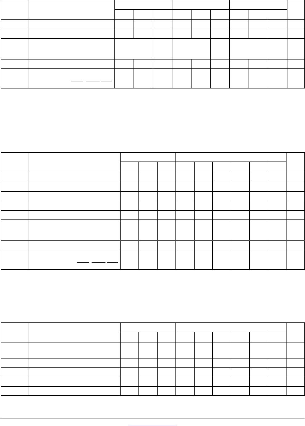
Table 5. 10EP DC CHARACTERISTICS, PECL V
CC
= 3.3 V, V
EE
= 0 V (Note 4)
Symbol
Characteristic
−40°C 25°C 85°C
Unit
Min Typ Max Min Typ Max Min Typ Max
I
EE
Negative Power Supply Current 105 125 145 105 125 145 105 125 145 mA
V
OH
Output HIGH Voltage (Note 5) 2165 2290 2415 2230 2355 2480 2290 2415 2540 mV
V
OL
Output LOW Voltage (Note 5) 1365 1490 1615 1430 1555 1680 1490 1615 1740 mV
V
IH
Input HIGH Voltage (Single−Ended) 2090 2415 2155 2480 2215 2540 mV
V
IL
Input LOW Voltage (Single−Ended) 1365 1690 1460 1755 1490 1815 mV
V
IHCMR
Input HIGH Voltage Common Mode
Range (Differential Configuration)
(Note 6)
2.0 3.3 2.0 3.3 2.0 3.3 V
I
IH
Input HIGH Current (@ V
IH
) 150 150 150
mA
I
IL
Input LOW Current (@ V
IL
)
CLK0, CLK1, D, S−IN
CLK0
, CLK1, S−IN
0.5
−150
0.5
−150
0.5
−150
mA
NOTE: Device will meet the specifications after thermal equilibrium has been established when mounted in a test socket or printed circuit
board with maintained transverse airflow greater than 500 lfpm.
4. Input and output parameters vary 1:1 with V
CC
. V
EE
can vary +0.3 V to −2.2 V.
5. All loading with 50 W to V
CC
− 2.0 V.
6. V
IHCMR
min varies 1:1 with V
EE
, V
IHCMR
max varies 1:1 with V
CC
. The V
IHCMR
range is referenced to the most positive side of the differential
input signal.
Table 6. 10EP DC CHARACTERISTICS, PECL V
CC
= 5.0 V, V
EE
= 0 V (Note 7)
−40°C 25°C 85°C
Symbol Characteristic Min Typ Max Min Typ Max Min Typ Max Unit
I
EE
Negative Power Supply Current (Note 8) 105 125 145 105 125 145 105 125 145 mA
V
OH
Output HIGH Voltage (Note 9) 3865 3990 4115 3930 4055 4180 3990 4115 4240 mV
V
OL
Output LOW Voltage (Note 9) 3065 3190 3315 3130 3255 3380 3190 3315 3440 mV
V
IH
Input HIGH Voltage (Single−Ended) 3790 4115 3855 4180 3915 4240 mV
V
IL
Input LOW Voltage (Single−Ended) 3065 3390 3130 3455 3190 3515 mV
V
IHCMR
Input HIGH Voltage Common Mode
Range (Differential Configuration)
(Note 10)
2.0 5.0 2.0 5.0 2.0 5.0 V
I
IH
Input HIGH Current (@ V
IH
) 150 150 150
mA
I
IL
Input LOW Current (@ V
IL
)
CLK0, CLK1, D, S−IN
CLK0
, CLK1, S−IN
0.5
−150
0.5
−150
0.5
−150
mA
NOTE: Device will meet the specifications after thermal equilibrium has been established when mounted in a test socket or printed circuit
board with maintained transverse airflow greater than 500 lfpm.
7. Input and output parameters vary 1:1 with V
CC
. V
EE
can vary +2.0 V to −0.5 V.
8. Required 500 lfpm air flow when using +5 V power supply. For (V
CC
− V
EE
) >3.3 V, 5 W to 10 W in line with V
EE
required for maximum thermal
protection at elevated temperatures. Recommend V
CC
− V
EE
operation at  3.3 V.
9. All loading with 50 W to V
CC
− 2.0 V.
10.V
IHCMR
min varies 1:1 with V
EE
, V
IHCMR
max varies 1:1 with V
CC
. The V
IHCMR
range is referenced to the most positive side of the differential
input signal.
Table 7. 10EP DC CHARACTERISTICS, NECL V
CC
= 0 V, V
EE
= −5.5 V to −3.0 V (Note 11)
−40°C 25°C 85°C
Symbol Characteristic Min Typ Max Min Typ Max Min Typ Max Unit
I
EE
Negative Power Supply Current
(Note 12)
105 125 145 105 125 145 105 125 145 mA
V
OH
Output HIGH Voltage (Note 13) −1135 −1010 −885 −1070 −945 −820 −1010 −885 −760 mV
V
OL
Output LOW Voltage (Note 13) −1935 −1810 −1685 −1870 −1745 −1620 −1810 −1685 −1560 mV
MC10EP142, MC100EP142
www.onsemi.com
8
Table 7. 10EP DC CHARACTERISTICS, NECL V
CC
= 0 V, V
EE
= −5.5 V to −3.0 V (Note 11)
85°C25°C−40°C
Symbol UnitMaxTypMinMaxTypMinMaxTypMinCharacteristic
V
IH
Input HIGH Voltage (Single−Ended) −1210 −885 −1145 −820 −1085 −760 mV
V
IL
Input LOW Voltage (Single−Ended) −1935 −1610 −1870 −1545 −1810 −1485 mV
V
IHCMR
Input HIGH Voltage Common Mode
Range (Differential Configuration)
(Note 14)
V
EE
+2.0 0.0 V
EE
+2.0 0.0 V
EE
+2.0 0.0 V
I
IH
Input HIGH Current (@ V
IH
) 150 150 150
mA
I
IL
Input LOW Current (@ V
IL
)
CLK0, CLK1, D, S−IN
CLK0
, CLK1, S−IN
0.5
−150
0.5
−150
0.5
−150
mA
NOTE: Device will meet the specifications after thermal equilibrium has been established when mounted in a test socket or printed circuit
board with maintained transverse airflow greater than 500 lfpm.
11. Input and output parameters vary 1:1 with V
CC
.
12.Required 500 lfpm air flow when using −5 V power supply. For (V
CC
− V
EE
) >3.3 V, 5 W to 10 W in line with V
EE
required for maximum thermal
protection at elevated temperatures. Recommend V
CC
−V
EE
operation at  3.3 V.
13.All loading with 50 W to V
CC
− 2.0 V.
14.V
IHCMR
min varies 1:1 with V
EE
, V
IHCMR
max varies 1:1 with V
CC
. The V
IHCMR
range is referenced to the most positive side of the differential
input signal.
Table 8. 100EP DC CHARACTERISTICS, PECL V
CC
= 3.3 V, V
EE
= 0 V (Note 15)
−40°C 25°C 85°C
Symbol Characteristic Min Typ Max Min Typ Max Min Typ Max Unit
I
EE
Negative Power Supply Current 105 125 145 105 130 150 105 130 150 mA
V
OH
Output HIGH Voltage (Note 16) 2155 2280 2405 2155 2280 2405 2155 2280 2405 mV
V
OL
Output LOW Voltage (Note 16) 1305 1480 1605 1305 1480 1605 1305 1480 1605 mV
V
IH
Input HIGH Voltage (Single−Ended) 2075 2420 2075 2420 2075 2420 mV
V
IL
Input LOW Voltage (Single−Ended) 1305 1675 1305 1675 1305 1675 mV
V
IHCMR
Input HIGH Voltage Common Mode
Range (Differential Configuration)
(Note 17)
2.0 3.3 2.0 3.3 2.0 3.3 V
I
IH
Input HIGH Current (@ V
IH
) 150 150 150
mA
I
IL
Input LOW Current (@ V
IL
)
CLK0, CLK1, D, S−IN
CLK0
, CLK1, S−IN
0.5
−150
0.5
−150
0.5
−150
mA
NOTE: Device will meet the specifications after thermal equilibrium has been established when mounted in a test socket or printed circuit
board with maintained transverse airflow greater than 500 lfpm.
15.Input and output parameters vary 1:1 with V
CC
. V
EE
can vary +0.3 V to −2.2 V.
16.All loading with 50 W to V
CC
− 2.0 V.
17.V
IHCMR
min varies 1:1 with V
EE
, V
IHCMR
max varies 1:1 with V
CC
. The V
IHCMR
range is referenced to the most positive side of the differential
input signal.
Table 9. 100EP DC CHARACTERISTICS, PECL V
CC
= 5.0 V, V
EE
= 0 V (Note 18)
−40°C 25°C 85°C
Symbol Characteristic Min Typ Max Min Typ Max Min Typ Max Unit
I
EE
Negative Power Supply Current
(Note 19)
105 125 145 105 130 150 105 130 150 mA
V
OH
Output HIGH Voltage (Note 20) 3855 3980 4105 3855 3980 4105 3855 3980 4105 mV
V
OL
Output LOW Voltage (Note 20) 3005 3180 3305 3005 3180 3305 3005 3180 3305 mV
V
IH
Input HIGH Voltage (Single−Ended) 3775 4120 3775 4120 3775 4120 mV
V
IL
Input LOW Voltage (Single−Ended) 3005 3375 3005 3375 3005 3375 mV
MC10EP142, MC100EP142
www.onsemi.com
9
Table 9. 100EP DC CHARACTERISTICS, PECL V
CC
= 5.0 V, V
EE
= 0 V (Note 18)
85°C25°C−40°C
Symbol UnitMaxTypMinMaxTypMinMaxTypMinCharacteristic
V
IHCMR
Input HIGH Voltage Common Mode
Range (Differential Configuration)
(Note 21)
2.0 5.0 2.0 5.0 2.0 5.0 V
I
IH
Input HIGH Current (@ V
IH
) 150 150 150
mA
I
IL
Input LOW Current (@ V
IL
)
CLK0, CLK1, D, S−IN
CLK0
, CLK1, S−IN
0.5
−150
0.5
−150
0.5
−150
mA
NOTE: Device will meet the specifications after thermal equilibrium has been established when mounted in a test socket or printed circuit
board with maintained transverse airflow greater than 500 lfpm.
18.Input and output parameters vary 1:1 with V
CC
. V
EE
can vary +2.0 V to −0.5 V.
19.Required 500 lfpm air flow when using +5 V power supply. For (V
CC
− V
EE
) >3.3 V, 5 W to 10 W in line with V
EE
required for maximum thermal
protection at elevated temperatures. Recommend V
CC
−V
EE
operation at  3.3 V.
20.All loading with 50 W to V
CC
− 2.0 V.
21.V
IHCMR
min varies 1:1 with V
EE
, V
IHCMR
max varies 1:1 with V
CC
. The V
IHCMR
range is referenced to the most positive side of the differential
input signal.
Table 10. 100EP DC CHARACTERISTICS, NECL V
CC
= 0 V, V
EE
= −5.5 V to −3.0 V (Note 22)
−40°C 25°C 85°C
Symbol Characteristic Min Typ Max Min Typ Max Min Typ Max Unit
I
EE
Negative Power Supply Current
(Note 23)
105 125 145 105 130 150 105 130 150 mA
V
OH
Output HIGH Voltage (Note 24) −1145 −1020 −895 −1145 −1020 −895 −1145 −1020 −895 mV
V
OL
Output LOW Voltage (Note 24) −1995 −1820 −1695 −1995 −1820 −1695 −1995 −1820 −1695 mV
V
IH
Input HIGH Voltage (Single−Ended) −1225 −880 −1225 −880 −1225 −880 mV
V
IL
Input LOW Voltage (Single−Ended) −1995 −1625 −1995 −1625 −1995 −1625 mV
V
IHCMR
Input HIGH Voltage Common Mode
Range (Differential Configuration)
(Note 25)
V
EE
+2.0 0.0 V
EE
+2.0 0.0 V
EE
+2.0 0.0 V
I
IH
Input HIGH Current (@ V
IH
) 150 150 150
mA
I
IL
Input LOW Current (@ V
IL
)
CLK0, CLK1, D, S−IN
CLK0
, CLK1, S−IN
0.5
−150
0.5
−150
0.5
−150
mA
NOTE: Device will meet the specifications after thermal equilibrium has been established when mounted in a test socket or printed circuit
board with maintained transverse airflow greater than 500 lfpm.
22.Input and output parameters vary 1:1 with V
CC
.
23.Required 500 lfpm air flow when using −5 V power supply. For (V
CC
− V
EE
) >3.3 V, 5 W to 10 W in line with V
EE
required for maximum thermal
protection at elevated temperatures. Recommend V
CC
−V
EE
operation at  3.3 V.
24.All loading with 50 W to V
CC
− 2.0 V.
25.V
IHCMR
min varies 1:1 with V
EE
, V
IHCMR
max varies 1:1 with V
CC
. The V
IHCMR
range is referenced to the most positive side of the differential
input signal.
Table 11. AC CHARACTERISTICS V
CC
= 3.0 V to 5.5 V; V
EE
= 0.0 V or V
CC
= 0.0 V; V
EE
= −3.0 V to −5.5 V (Note 26)
Symbol
Characteristic
−40°C 25°C 85°C
Unit
Min Typ Max Min Typ Max Min Typ Max
f
SHIFT
Maximum Shift Frequency 2.8 GHz
t
PLH
,
t
PHL
Propagation Delay to Output
CLKx
MR
500
500
625
625
750
750
550
550
675
675
800
800
575
575
700
700
825
825
ps
t
s
Setup Time
D
SEL
50
100
−50
50
50
100
−50
50
50
100
−50
50
ps

MC100EP142FAG

Mfr. #:
Manufacturer:
ON Semiconductor
Description:
Counter Shift Registers 3.3V/5V ECL 9-Bit Shift
Lifecycle:
New from this manufacturer.
Delivery:
DHL FedEx Ups TNT EMS
Payment:
T/T Paypal Visa MoneyGram Western Union