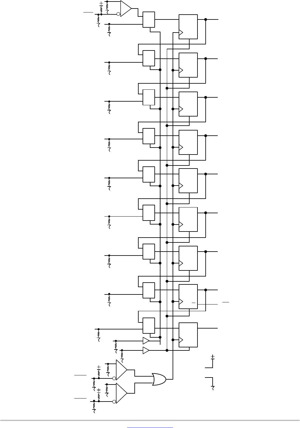
MC10EP142, MC100EP142
www.onsemi.com
6
Table 4. MAXIMUM RATINGS
Symbol Parameter Condition 1 Condition 2 Rating Unit
V
CC
Positive Power Supply V
EE
= 0 V 8 V
V
EE
Negative Power Supply V
CC
= 0 V −8 V
V
I
PECL Mode Input Voltage
NECL Mode Input Voltage
V
EE
= 0 V
V
CC
= 0 V
V
I
v V
CC
V
I
w V
EE
6
−6
V
I
out
Output Current Continuous
Surge
50
100
mA
T
A
Operating Temperature Range −40 to +85 °C
T
stg
Storage Temperature Range −65 to +150 °C
q
JA
Thermal Resistance (Junction−to−Ambient) 0 lfpm
500 lfpm
LQFP−32
LQFP−32
80
55
°C/W
q
JC
Thermal Resistance (Junction−to−Case) Standard Board LQFP−32 12 to 17 °C/W
q
JA
Thermal Resistance (Junction−to−Ambient) 0 lfpm
500 lfpm
QFN−32
QFN−32
31
27
°C/W
q
JC
Thermal Resistance (Junction−to−Case) 2S2P QFN−32 12 °C/W
T
sol
Wave Solder Pb−Free v3 sec @ 260°C 265 °C
Stresses exceeding those listed in the Maximum Ratings table may damage the device. If any of these limits are exceeded, device functionality
should not be assumed, damage may occur and reliability may be affected.