LTC6993-1/LTC6993-2
LTC6993-3/LTC6993-4
10
69931234fc
For more information www.linear.com/LTC6993-1
pin FuncTions
(DCB/S6)
V
+
(Pin 1/Pin 5): Supply Voltage (2.25V to 5.5V). This
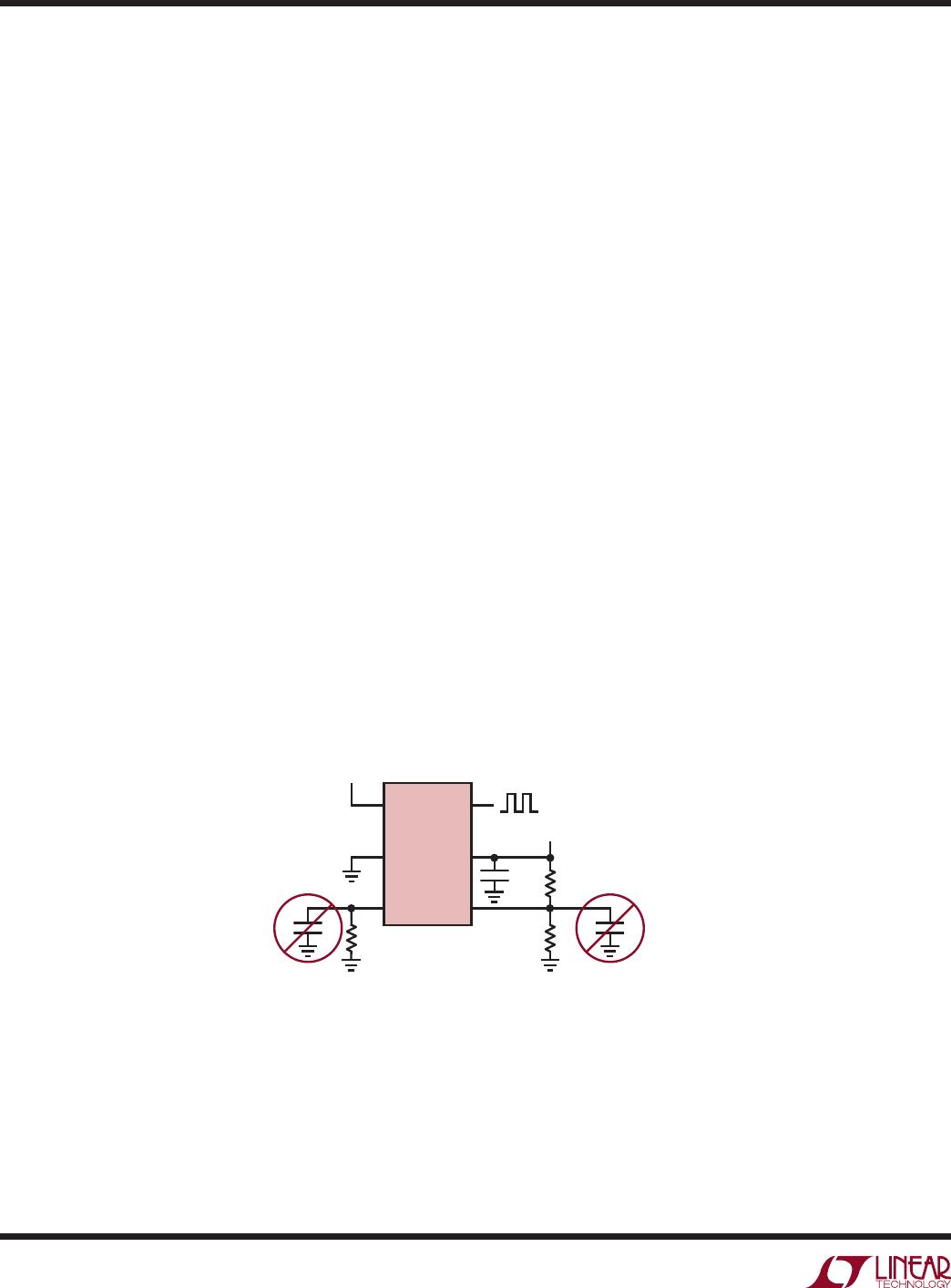
supply should be kept free from noise and ripple. It should
be bypassed directly to the GND pin with a 0.1µF capacitor.
DIV (Pin 2/Pin 4): Programmable Divider and Polarity
Input. The DIV pin voltage (V
DIV
) is internally converted
into a 4-bit result (DIVCODE). V
DIV
may be generated by
a resistor divider between V
+
and GND. Use 1% resistors
to ensure an accurate result. The DIV pin and resistors
should be shielded from the OUT pin or any other traces
that have fast edges. Limit the capacitance on the DIV pin
to less than 100pF so that V
DIV
settles quickly. The MSB of
DIVCODE (POL) determines the polarity of the OUT pins.
When POL = 0 the output produces a positive pulse. When
POL = 1 the output produces a negative pulse.
SET (Pin 3/Pin 3): Pulse Width Setting Input. The voltage
on the SET pin (V
SET
) is regulated to 1V above GND. The
amount of current sourced from the SET pin (I
SET
) pro-
grams the master oscillator frequency. The I
SET
current
range is 1.25µA to 20µA. The output pulse will continue
indefinitely if I
SET
drops below approximately 500nA,
and will terminate when I
SET
increases again. A resistor
connected between SET and GND is the most accurate
way to set the pulse width. For best performance, use
a precision metal or thin film resistor of 0.5% or better
tolerance and 50ppm/°C or better temperature coefficient.
For lower accuracy applications an inexpensive 1% thick
film resistor may be used.
Limit the capacitance on the SET pin to less than 10pF
to minimize jitter and ensure stability. Capacitance less
than 100pF maintains the stability of the feedback circuit
regulating the V
SET
voltage.
TRIG (Pin 4/Pin 1): Trigger Input. Depending on the ver-
sion, a rising or falling edge on TRIG will initiate the output
pulse. LT
C6993
-1 and LTC6993-2 are rising-edge sensi-
tive. L
TC6993-
3 and LTC6993-4 are falling-edge sensitive.
The LTC6993-2 and LTC6993-4 are retriggerable, allowing
the pulse width to be extended by additional trigger signals
that occur while the output is active. The LTC6993-1/
LTC6993-3 will ignore additional trigger inputs until the
output pulse has terminated.
GND (Pin 5/Pin 2): Ground. Tie to a low inductance ground
plane for best performance.
OUT (Pin 6/Pin 6): Output. The OUT pin swings from
GND to V
+
with an output resistance of approximately
30Ω. When driving an LED or other low impedance load
a series output resistor should be used to limit source/
sink current to 20mA.
69931234 PF
LTC6993
TRIG
GND
SET
OUT
V
+
DIV
C1
0.1µF
R
SET
R2
R1
V
+
V
+
LTC6993-1/LTC6993-2
LTC6993-3/LTC6993-4
11
69931234fc
For more information www.linear.com/LTC6993-1
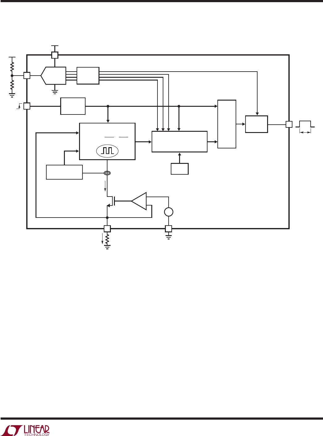
block DiagraM
(S6 package pin numbers shown)
69931234 BD
PROGRAMMABLE DIVIDER
÷1, 8, 64, 512, 4096,
2
15
, 2
18
, 2
21
MASTER OSCILLATOR
POR
DIGITAL
FILTER
4-BIT A/D
CONVERTER
POL
R1
R2
DIV
V
+
OUT
5
4
TRIG
1
6
HALT OSCILLATOR
IF I
SET
< 500nA
MCLK
+
I
SET
I
SET
V
SET
= 1V
+
1V
3 22
GND
SET
R
SET
t
OUT
TRIGGER/
RETRIGGER
LOGIC
t
MASTER
=
s
50kΩ
V
SET
I
SET
S
R
Q
OUTPUT
POLARITY
LTC6993-1/LTC6993-2
LTC6993-3/LTC6993-4
12
69931234fc
For more information www.linear.com/LTC6993-1
operaTion
The LTC6993 is built around a master oscillator with a 1µs
minimum period. The oscillator is controlled by the SET
pin current (I
SET
) and voltage (V
SET
), with a 1µs/50kΩ
conversion factor that is accurate to ±1.7% under typical
conditions.
t
MASTER
=
1µs
50kΩ
V
SET
I
SET
A feedback loop maintains V
SET
at 1V ±30mV, leaving
I
SET
as the primary means of controlling the pulse width.
The simplest way to generate I
SET
is to connect a resistor
(R
SET
) between SET and GND, such that I
SET
= V
SET
/R
SET
.
The master oscillator equation reduces to:
t
MASTER
= 1µs
R
SET
50kΩ
From this equation, it is clear that V
SET
drift will not affect
the pulse width when using a single program resistor
(R
SET
). Error sources are limited to R
SET
tolerance and
the inherent pulse width accuracy t
OUT
of the LTC6993.
R
SET
may range from 50k to 800k (equivalent to I
SET
between 1.25µA and 20µA).
A trigger signal (rising or falling edge on TRIG pin) latches
the output to the active state, beginning the output pulse. At
the same time, the master oscillator is enabled to time the
duration of the output pulse. When the desired pulse width
is reached, the master oscillator resets the output latch.
The LTC6993 also includes a programmable frequency
divider which can further divide the frequency by 1, 8, 64,
512, 4096, 2
15
, 2
18
or 2
21
. This extends the pulse width
duration by those same factors. The divider ratio N
DIV
is
set by a resistor divider attached to the DIV pin.
t
OUT
=
N
DIV
50kΩ
V
SET
I
SET
1µ
s
With R
SET
in place of V
SET
/I
SET
the equation reduces to:
t
OUT
=
N
DIV
R
SET
50kΩ
1µ
s
DIVCODE
The DIV pin connects to an internal, V
+
referenced 4-bit A/D
converter that determines the DIVCODE value. DIVCODE
programs two settings on the LTC6993:
1. DIVCODE determines the frequency divider setting,
N
DIV
.
2. DIVCODE determines the polarity of OUT pin, via the
POL bit.
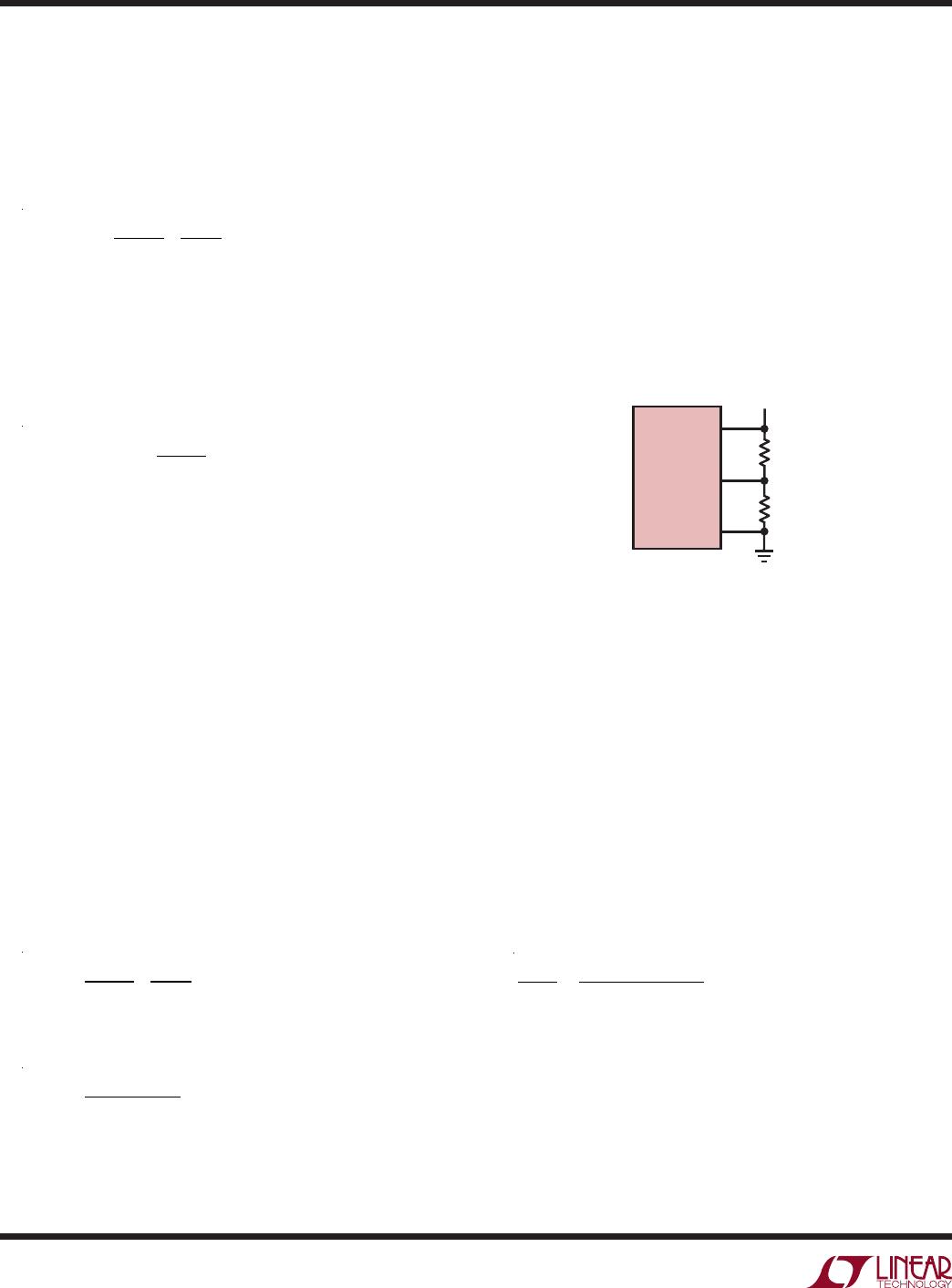
V
DIV
may be generated by a resistor divider between V
+
and GND as shown in Figure 1.
Figure 1. Simple Technique for Setting DIVCODE
69931234 F01
LTC6993
V
+
DIV
GND
R1
R2
2.25V TO 5.5V
Table 1 offers recommended 1% resistor values that ac-
curately produce the correct voltage division as well as the
corresponding N
DIV
and POL values for the recommended
resistor pairs. Other values may be used as long as:
1. The V
DIV
/V
+
ratio is accurate to ±1.5% (including resis-
tor tolerances and temperature effects).
2.
The driving impedance (R1||R2) does not exceed 500kΩ.
If the voltage is generated by other means (i.e., the output
of a DAC) it must track the V
+
supply voltage. The last
column in Table 1 shows the ideal ratio of V
DIV
to the
supply voltage, which can also be calculated as:
V
DIV
V
+
=
DIVCODE
+
0.5
16
±1.5%
For example, if the supply is 3.3V and the desired DIVCODE
is 4, V
DIV
= 0.281 3.3V = 928mV ± 50mV.
Figure 2 illustrates the information in Table 1, showing
that N
DIV
is symmetric around the DIVCODE midpoint.
LTC6993HDCB-1#TRPBF

Mfr. #:
Manufacturer:
Analog Devices Inc.
Description:
Monostable Multivibrator One Shot with Rising Edge Trigger, Non-Retriggerable
Lifecycle:
New from this manufacturer.
Delivery:
DHL FedEx Ups TNT EMS
Payment:
T/T Paypal Visa MoneyGram Western Union