LTC6993-1/LTC6993-2
LTC6993-3/LTC6993-4
16
69931234fc
For more information www.linear.com/LTC6993-1
applicaTions inForMaTion
Basic Operation
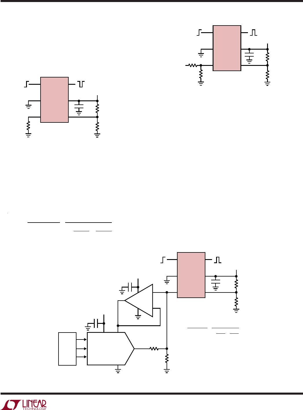
The simplest and most accurate method to program
the LTC6993 is to use a single resistor, R
SET
, between
the SET and GND pins. The design procedure is a four
step process. Alternatively, Linear Technology offers the
easy-to-use TimerBlox Designer tool to quickly design
any LTC6993 based circuit. Download the free TimerBlox
Designer software at www.linear.com/timerblox.
Step 1: Select the POL Bit Setting.
The LTC6993 can generate positive or negative output
pulses, depending on the setting of the POL bit. The POL
bit is the DIVCODE MSB, so any DIVCODE 8 has POL = 1
and produces active-low pulses.
Step 2: Select LTC6993 Version.
Two input-related choices dictate the proper LTC6993 for
a given application:
Is TRIG a rising or falling-edge input?
Should retriggering be allowed?
Use Table 2 to select a particular variety of LTC6993.
Step 3: Select the N
DIV
Frequency Divider Value.
As explained earlier, the voltage on the DIV pin sets the
DIVCODE which determines both the POL bit and the N
DIV
value. For a given output pulse width (t
OUT
), N
DIV
should
be selected to be within the following range:
t
OUT
16µs
N
DIV
t
OUT
1µs
(1)
To minimize supply current, choose the lowest N
DIV
value.
However, in some cases a higher value for N
DIV
will provide
better accuracy (see Electrical Characteristics).
Table 1 can also be used to select the appropriate N
DIV
values for the desired t
OUT
.
With POL already chosen, this completes the selection of
DIVCODE. Use Table 1 to select the proper resistor divider
or V
DIV
/V
+
ratio to apply to the DIV pin.
Step 4: Calculate and Select R
SET
.
The final step is to calculate the correct value for R
SET
using the following equation:
R
SET
=
50k
1µs
t
OUT
N
DIV
(2)
Select the standard resistor value closest to the calculated
value.
Example: Design a one-shot circuit that satisfies the fol-
lowing requirements:
t
OUT
= 100µs
Negative Output Pulse
Rising-Edge Trigger Input
Retriggerable Input
Minimum power consumption
Step 1: Select the POL Bit Setting.
For inverted (negative) output pulse, choose POL = 1.
Step 2: Select the LTC6993 Version.
A rising-edge retriggerable input requires the LTC6993-2.
Step 3: Select the N
DIV
Frequency Divider Value.
Choose an N
DIV
value that meets the requirements of
Equation (1), using t
OUT
= 100µs:
6.25 ≤ N
DIV
≤ 100
Potential settings for N
DIV
include 8 and 64. N
DIV
= 8 is
the best choice, as it minimizes supply current by us-
ing a large R
SET
resistor. POL = 1 and N
DIV
= 8 requires
DIVCODE = 14. Using T
able 1, choose R1 = 102k and
R2 = 976k values to program DIVCODE = 14.
Step 4: Select R
SET
.
Calculate the correct value for R
SET
using Equation (2):
R
SET
=
50k
1µs
100µs
8
= 625k
LTC6993-1/LTC6993-2
LTC6993-3/LTC6993-4
17
69931234fc
For more information www.linear.com/LTC6993-1
Since 625k is not available as a standard 1% resistor,
substitute 619k if a 0.97% shift in t
OUT
is acceptable.
Otherwise, select a parallel or series pair of resistors such
as 309k and 316k to attain a more precise resistance.
The completed design is shown in Figure 7.
applicaTions inForMaTion
Figure 7. 100µs Negative Pulse Generator
LTC6993-2
TRIG
GND
SET
OUT
V
+
DIV
R1
102k
DIVCODE = 14
69931234 F07
2.25V TO 5.5V
R2
976k
0.1µF
R
SET
625k
Figure 8. Voltage-Controlled Pulse Width
LTC6993
TRIG
GND
SET
OUT
V
+
DIV
R1
C1
0.1µF
69931234 F08
V
+
R2
R
SET
R
MOD
V
CTRL
69931234 F09
LTC6993
TRIG
GND
SET
OUT
V
+
DIV
C1
0.1µF
R1
R2
V
+
R
MOD
R
SET
+
V
+
0.1µF
1/2
LTC6078
LTC1659
V
+
V
CC
REF
GND
V
OUT
µP
D
IN
CLK
CS/LD
N
DIV
• R
MOD
50kΩ
t
OUT
=
D
IN
= 0 TO 4095
1+
R
MOD
R
SET
D
IN
4096
s
0.1µF
Voltage-Controlled Pulse Width
With one additional resistor, the LTC6993 output pulse
width can be manipulated by an external voltage. As shown
in Figure 8, voltage V
CTRL
sources/sinks a current through
R
MOD
to vary the I
SET
current, which in turn modulates
the pulse width as described in Equation (3).
t
OUT
=
N
DIV
R
MOD
50kΩ
1µs
1+
R
MOD
R
SET
V
CTRL
V
SET
(3)
Digital Pulse Width Control
The control voltage can be generated by a DAC (digital-to-
analog converter), resulting in a digitally-controlled pulse
width. Many DACs allow for the use of an external refer
-
ence. If such a DAC is used to provide the V
CTRL
voltage,
the V
SET
dependency can be eliminated by buffering V
SET
and using it as the DACs reference voltage, as shown in
Figure 9. The DACs output voltage now tracks any V
SET
variation and eliminates it as an error source. The SET pin
cannot be tied directly to the reference input of the DAC
because the current drawn by the DACs REF input would
affect the pulse width.
Figure 9. Digitally Controlled Pulse Width
LTC6993-1/LTC6993-2
LTC6993-3/LTC6993-4
18
69931234fc
For more information www.linear.com/LTC6993-1
I
SET
Extremes (Master Oscillator Frequency Extremes)
When operating with I
SET
outside of the recommended
1.25µA to 20µA range, the master oscillator operates
outside of the 62.5kHz to 1MHz range in which it is most
accurate.
The oscillator will still function with reduced accuracy for
I
SET
< 1.25µA. At approximately 500nA, the oscillator will
stop. Under this condition, the output pulse can still be
initiated, but will not terminate until I
SET
increases and
the master oscillator starts again.
At the other extreme, it is not recommended to operate
the master oscillator beyond 2MHz because the accuracy
of the DIV pin ADC will suffer.
Settling Time
Following a 2× or 0.5× step change in I
SET
, the output
pulse width takes approximately six master clock cycles
(6
t
MASTER
) to settle to within 1% of the final value. An
example is shown in Figure 10, using the circuit in Figure 8.
Coupling Error
The current sourced by the SET pin is used to bias the in
-
ternal master oscillator. The LT
C6993 responds to changes
in I
SET
almost immediately, which provides excellent
settling time. However, this fast response also makes the
SET pin sensitive to coupling from digital signals, such
as the TRIG input.
Even an excellent layout will allow some coupling between
TRIG and SET. Additional error is included in the speci
-
fied accuracy for N
DIV
= 1 to account for this. Figure 11
shows that ÷1 supply variation is dependent on coupling
from rising or falling trigger inputs and, to a lesser extent,
output polarity.
A very poor layout can actually degrade performance
further. The PCB layout should avoid routing SET next to
TRIG (or any other fast-edge, wide-swing signal).
applicaTions inForMaTion
Figure 10. Typical Settling Time
V
CTRL
2V/DIV
TRIG
5V/DIV
OUT
5V/DIV
PULSE WIDTH
2µs/DIV
LTC6993-1
V
+
= 3.3V
DIVCODE = 0
R
SET
= 200k
R
MOD
= 464k
t
OUT
= 3µs AND 6µs
20µs/DIV
69931234 F10
SUPPLY (V)
2
–1.0
DRIFT (%)
–0.8
–0.4
–0.2
0
1.0
0.4
3
4
69931234 F11
–0.6
0.6
0.8
0.2
5
6
R
SET
= 50k
N
DIV
= 1
LTC6993-1
POL = 0
LTC6993-1
POL = 1
LTC6993-3
POL = 1
LTC6993-3
POL = 0
Figure 11. t
OUT
Drift vs Supply Voltage

LTC6993HDCB-1#TRPBF

Mfr. #:
Manufacturer:
Analog Devices Inc.
Description:
Monostable Multivibrator One Shot with Rising Edge Trigger, Non-Retriggerable
Lifecycle:
New from this manufacturer.
Delivery:
DHL FedEx Ups TNT EMS
Payment:
T/T Paypal Visa MoneyGram Western Union