NTHL040N65S3F

© Semiconductor Components Industries, LLC, 2017
May, 2018 Rev. 6
1 Publication Order Number:
NTHL040N65S3F/D
NTHL040N65S3F
Power MOSFET, N-Channel,
SUPERFET
)
III, FRFET
)
,
650 V, 65 A, 40 mW
Description
SUPERFET III MOSFET is ON Semiconductors brandnew high
voltage superjunction (SJ) MOSFET family that is utilizing charge
balance technology for outstanding low on-resistance and lower gate
charge performance. This advanced technology is tailored to minimize
conduction loss, provide superior switching performance, and
withstand extreme dv/dt rate.
Consequently, SUPERFET III MOSFET is very suitable for the
various power system for miniaturization and higher efficiency.
SUPERFET III FRFET
MOSFET’s optimized reverse recovery
performance of body diode can remove additional component and
improve system reliability.
Features
700 V @ T
J
= 150°C
Typ. R
DS(on)
= 32 mW
Ultra Low Gate Charge (Typ. Q
g
= 158 nC)
Low Effective Output Capacitance (Typ. C
oss(eff.)
= 1366 pF)
100% Avalanche Tested
These Devices are PbFree and are RoHS Compliant
Applications
Telecom / Server Power Supplies
Industrial Power Supplies
EV Charger
UPS / Solar
TO247 long leads
CASE 340CH
See detailed ordering and shipping information on page 2 of
this data sheet.
ORDERING INFORMATION
www.onsemi.com
D
S
G
$Y = ON Semiconductor Logo
&Z = Assembly Plant Code
&3 = Data Code (Year & Week)
&K = Lot
NTHL040N65S3F = Specific Device Code
MARKING DIAGRAM
D
G
S
V
DSS
R
DS(ON)
MAX I
D
MAX
650 V
40 mW @ 10 V
65 A
$Y&Z&3&K
NTHL
040N65S3F
NTHL040N65S3F
www.onsemi.com
2
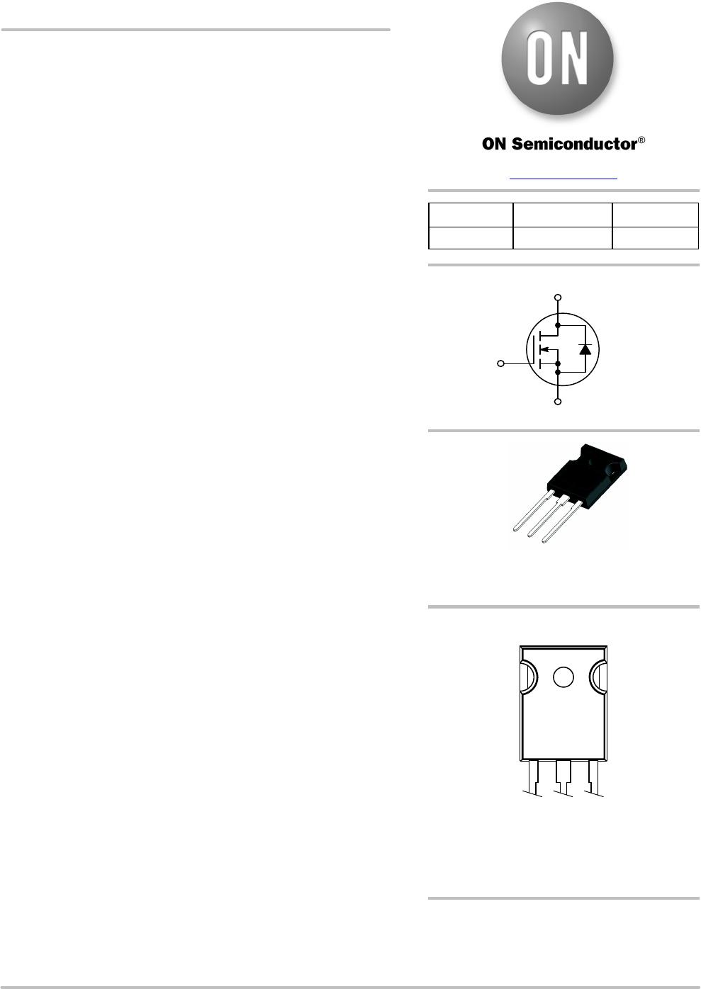
ABSOLUTE MAXIMUM RATINGS (T
C
= 25°C, Unless otherwise noted)
Symbol
Parameter NTHL040N65S3F Unit
V
DSS
Drain to Source Voltage 650 V
V
GSS
Gate to Source Voltage
DC ±30
V
AC (f > 1 Hz) ±30
I
D
Drain Current
Continuous (T
C
= 25°C) 65
A
Continuous (T
C
= 100°C) 45
I
DM
Drain Current Pulsed (Note 1) 162.5 A
E
AS
Single Pulsed Avalanche Energy (Note 2) 1009 mJ
I
AS
Avalanche Current (Note 2) 9 A
E
AR
Repetitive Avalanche Energy (Note 1) 4.46 mJ
dv/dt
MOSFET dv/dt 100
V/ns
Peak Diode Recovery dv/dt (Note 3) 50
P
D
Power Dissipation
(T
C
= 25°C) 446 W
Derate Above 25°C 3.57 W/°C
T
J
, T
STG
Operating and Storage Temperature Range 55 to +150 °C
T
L
Maximum Lead Temperature for Soldering, 1/8 from Case for 5 seconds 300 °C
Stresses exceeding those listed in the Maximum Ratings table may damage the device. If any of these limits are exceeded, device functionality
should not be assumed, damage may occur and reliability may be affected.
1. Repetitive rating: pulsewidth limited by maximum junction temperature.
2. I
AS
= 9 A, R
G
= 25 W, starting T
J
= 25°C.
3. I
SD
32.5 A, di/dt 200 A/ms, V
DD
400 V, starting T
J
= 25°C.
THERMAL CHARACTERISTICS
Symbol Parameter NTHL040N65S3F Unit
R
q
JC
Thermal Resistance, Junction to Case, Max. 0.28 _C/W
R
q
JA
Thermal Resistance, Junction to Ambient, Max. 40
PACKAGE MARKING AND ORDERING INFORMATION
Part Number Top Marking Package Packing Method Reel Size Tape Width Quantity
NTHL040N65S3F NTHL040N65S3F TO247 Tube N/A N/A 30 Units
NTHL040N65S3F
www.onsemi.com
3
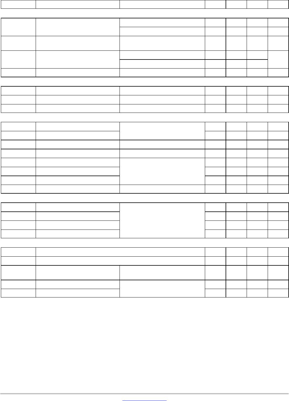
ELECTRICAL CHARACTERISTICS (T
C
= 25°C unless otherwise noted)
Symbol
Parameter Test Conditions Min. Typ. Max. Unit
OFF CHARACTERISTICS
BV
DSS
Drain to Source Breakdown Voltage
V
GS
=0V, I
D
= 1 mA, T
J
=25_C
650 V
V
GS
=0V, I
D
= 1 mA, T
J
= 150_C
700 V
DBV
DSS
/DT
J
Breakdown Voltage Temperature
Coefficient
I
D
= 15 mA, Referenced to 25_C
0.63
V/_C
I
DSS
Zero Gate Voltage Drain Current
V
DS
= 650 V, V
GS
=0V 10 mA
V
DS
= 520 V, T
C
= 125_C
213
I
GSS
Gate to Body Leakage Current V
GS
= ±30 V, V
DS
=0V ±100 nA
ON CHARACTERISTICS
V
GS(th)
Gate Threshold Voltage V
GS
=V
DS
, I
D
= 6.5 mA 3.0 5.0 V
R
DS(on)
Static Drain to Source On Resistance V
GS
=10V, I
D
= 32.5 A 32 40
mW
g
FS
Forward Transconductance V
DS
=20V, I
D
= 32.5 A 48 S
DYNAMIC CHARACTERISTICS
C
iss
Input Capacitance
V
DS
= 400 V, V
GS
= 0 V, f = 1 MHz
5940 pF
C
oss
Output Capacitance 140 pF
C
oss(eff.)
Effective Output Capacitance V
DS
= 0 V to 400 V, V
GS
=0V 1366 pF
C
oss(er.)
Energy Related Output Capacitance V
DS
= 0 V to 400 V, V
GS
=0V 247 pF
Q
g(tot)
Total Gate Charge at 10V
V
DS
= 400 V, I
D
= 32.5 A, V
GS
=10V
(Note 4)
158 nC
Q
gs
Gate to Source Gate Charge 48 nC
Q
gd
Gate to Drain “Miller” Charge 60 nC
ESR Equivalent Series Resistance f = 1 MHz 1.1
W
SWITCHING CHARACTERISTICS
t
d(on)
Turn-On Delay Time
V
DD
= 400 V, I
D
= 32.5 A,
V
GS
=10V, R
g
= 2.2 W
(Note 4)
41 ns
t
r
Turn-On Rise Time 41 ns
t
d(off)
Turn-Off Delay Time 101 ns
t
f
Turn-Off Fall Time 29 ns
SOURCE-DRAIN DIODE CHARACTERISTICS
I
S
Maximum Continuous Source to Drain Diode Forward Current 65 A
I
SM
Maximum Pulsed Source to Drain Diode Forward Current 162.5 A
V
SD
Source to Drain Diode Forward
Voltage
V
GS
=0V, I
SD
= 32.5 A 1.3 V
t
rr
Reverse Recovery Time
V
GS
=0V, I
SD
= 32.5 A,
dI
F
/dt = 100 A/ms
145 ns
Q
rr
Reverse Recovery Charge 737 nC
Product parametric performance is indicated in the Electrical Characteristics for the listed test conditions, unless otherwise noted. Product
performance may not be indicated by the Electrical Characteristics if operated under different conditions.
4. Essentially independent of operating temperature typical characteristics.
NTHL040N65S3F

Mfr. #:
Manufacturer:
ON Semiconductor
Description:
MOSFET SUPERFET3 650V TO247
Lifecycle:
New from this manufacturer.
Delivery:
DHL FedEx Ups TNT EMS
Payment:
T/T Paypal Visa MoneyGram Western Union

Products related to this Datasheet