Expand menu
Hello, Sign in
My Account
0
Cart
Home
Products
Sensors
Semiconductors
Passive Components
Connectors
Power
Electromechanical
Optoelectronics
Circuit Protection
Integrated Circuits - ICs
Main Products
Manufacturers
Blog
Services
About OMO
About Us
Contact Us
Check Stock
NTHL040N65S3F
P1-P3
P4-P6
P7-P9
P10-P11
NTHL040N65S3F
www
.onsemi.com
7
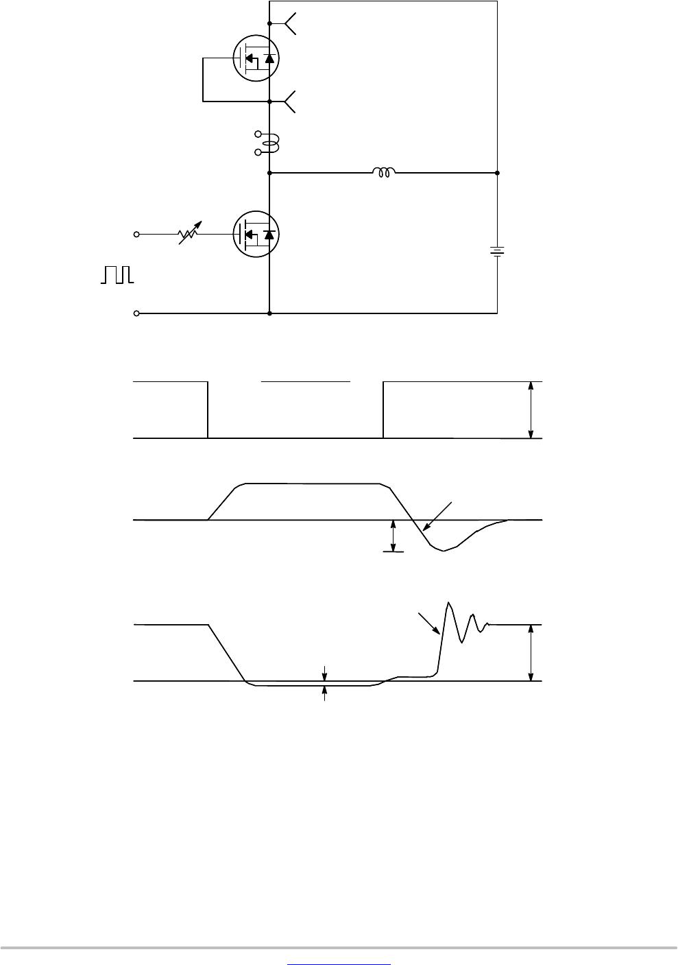
Figure 13. Gate Charge T
est Circuit & Waveform
Figure 14. Resistive Switching T
est Circuit & Waveforms
Figure 15. Unclamped Inductive Switching T
est Circuit & Waveforms
R
L
V
DS
V
GS
V
GS
R
G
DUT
V
DD
V
DS
V
GS
10%
90%
10%
90%
90%
t
on
t
off
t
r
t
f
t
d(on)
t
d(off)
Q
g
Q
gd
Q
gs
V
GS
Charge
V
DS
V
GS
R
L
DUT
I
G
= Const.
V
DD
V
DS
R
G
DUT
V
GS
L
I
D
t
p
V
DD
t
p
T
ime
I
AS
BV
DSS
I
D
(t)
V
DS
(t)
E
AS
+
1
2
@
LI
AS
2
NTHL040N65S3F
www
.onsemi.com
8
Figure 16. Peak Diode Recovery dv/dt T
est Circuit & Waveforms
DUT
L
V
DD
R
G
I
SD
V
SD
+
−
V
GS
Same T
ype
as DUT
−
dv/dt controlled by R
G
−
I
SD
controlled by pulse period
Driver
V
GS
(Driver)
I
SD
(DUT)
V
DS
(DUT)
V
SD
I
RM
10 V
di/dt
V
DD
I
FM
, Body Diode Forward Current
Body Diode Reverse Current
Body Diode Recovery dv/dt
Body Diode
Forward V
oltage Drop
D
+
Gate Pulse Width
Gate Pulse Period
SUPERFET is a registered trademark of Semiconductor Components Industries, LLC (SCILLC) or its subsidiaries in the United States and/or
other countries.
FRFET is a registered trademark of Semiconductor Components Industries, LLC (SCILLC) or its subsidiaries in the United States and/or other
countries.
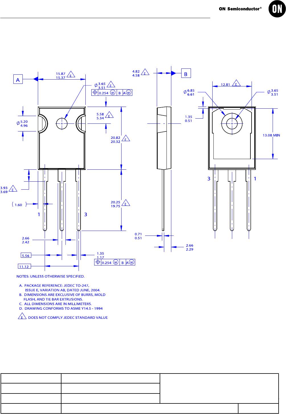
TO−247−3LD
CASE 340CH
ISSUE O
DA
TE 31 OCT 201
6
MECHANICAL CASE OUTLINE
P
ACKAGE DIMENSIONS
http://onsemi.com
1
©
Semiconductor Components Industries, LLC, 2002
October
, 2002 − Rev
. 0
Case Outline Number:
XXX
DOCUMENT NUMBER:
ST
A
TUS:
NEW ST
ANDARD:
DESCRIPTION:
98AON13853G
ON SEMICONDUCTOR ST
ANDARD
TO−247−3LD
Electronic
versions
are
uncontrolled
except
when
accessed
directly
from
the
Document
Repository
.
Printed
versions
are
uncontrolled
except
when
stamped
“CONTROLLED
COPY”
in
red.
P
AGE
1 OF 2
P1-P3
P4-P6
P7-P9
P10-P11
NTHL040N65S3F
Mfr. #:
Buy NTHL040N65S3F
Manufacturer:
ON Semiconductor
Description:
MOSFET SUPERFET3 650V TO247
Lifecycle:
New from this manufacturer.
Delivery:
DHL
FedEx
Ups
TNT
EMS
Payment:
T/T
Paypal
Visa
MoneyGram
Western
Union
Products related to this Datasheet
NTHL040N65S3F