LTC3625/LTC3625-1
6
3625f
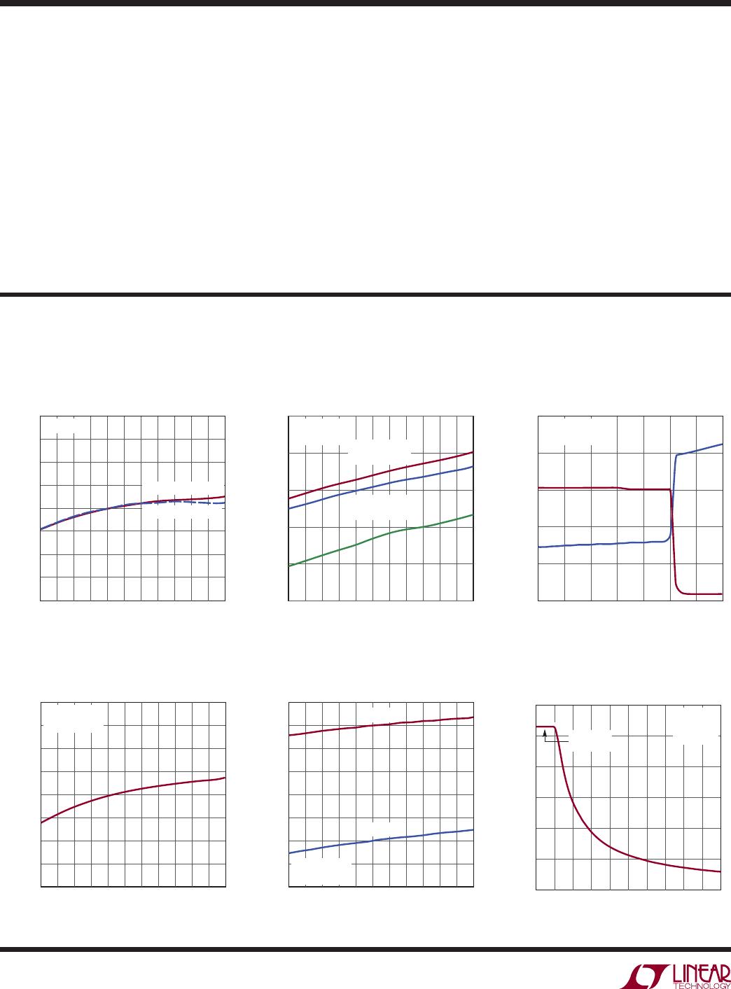
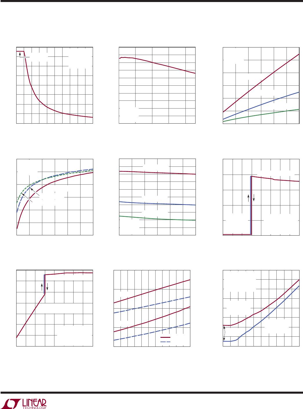
Typical perForMance characTerisTics
T
A
= 25°C, L1 = 3.3µH, L2 = 3.3µH, C
IN
= 10µF, C
TOP
= C
BOT
, LTC3625 unless otherwise specified.
SW1 (Pin 1): Switch Pin for the Buck Regulator. External
inductor connects between SW1 pin and V
MID
.
V
IN
(Pin 2): Input Voltage Pin. Bypass to GND with a 10µF
or larger ceramic capacitor.
CTL (Pin 3): Logic Input. CTL sets the charge mode of the
LTC3625/LTC3625-1. A logic high at CTL programs the part
to operate with a single inductor; a logic low programs
the part to operate with two inductors. In the 2-inductor
application the capacitor stack will charge approximately
twice as quickly. CTL is a high impedance input and must
be tied to either V
IN
or GND. Do not float.
V
SEL
(Pin 4): Logic Input. V
SEL
selects the output volt-
age of the LTC3625/LTC3625-1. A logic low at V
SEL
sets
the per-cell maximum voltage to 2.45V/2.05V (V
OUT
=
4.8V/4.0V); a logic high sets the per-cell maximum volt-
age to 2.70V/2.30V (V
OUT
= 5.3V/4.5V). When the part is
enabled, V
SEL
has a 4.5MΩ internal pull-down resistor; if
EN is low, then V
SEL
is a high impedance input pin.
EN (Pin 5): Logic Input. Enables the LTC3625/LTC3625-1.
Active high. Has a 4.5MΩ internal pull-down resistor.
Charge Profile Into Matched
SuperCaps Charge Profile with C
BOT
> C
TOP
Charge Profile with C
TOP
> C
BOT
pin FuncTions
PROG (Pin 6): Charge Current Program Pin. Connecting a
resistor from PROG to ground programs the buck output
current. This pin servos to 1.2V.
PFI (Pin 7): Input to the Power Fail Comparator. This pin
connects to an external resistor divider between V
IN
and
GND. If this functionality is not desired, PFI should be
tied to V
IN
.
PFO (Pin 8): Open-Drain Output of the Power-Fail Compara-
tor. The part pulls this pin low if V
IN
is less than a value
programmed by an external divider. This pin is active low
in shutdown mode. If this functionality is not desired PFO
should be left unconnected.
PGOOD (Pin 9): Logic Output. This is an open-drain
output which indicates that V
OUT
has settled to its final
value. Upon start-up, this pin remains low until the output
voltage, V
OUT
, is within 92.5% (typical) of its final value.
Once V
OUT
is valid, PGOOD becomes high impedance. If
V
OUT
falls to 89.5% (typical) of its correct regulation level,
PGOOD is pulled low. PGOOD may be pulled up through
an external resistor to an appropriate reference level. This
pin is active low in shutdown mode.
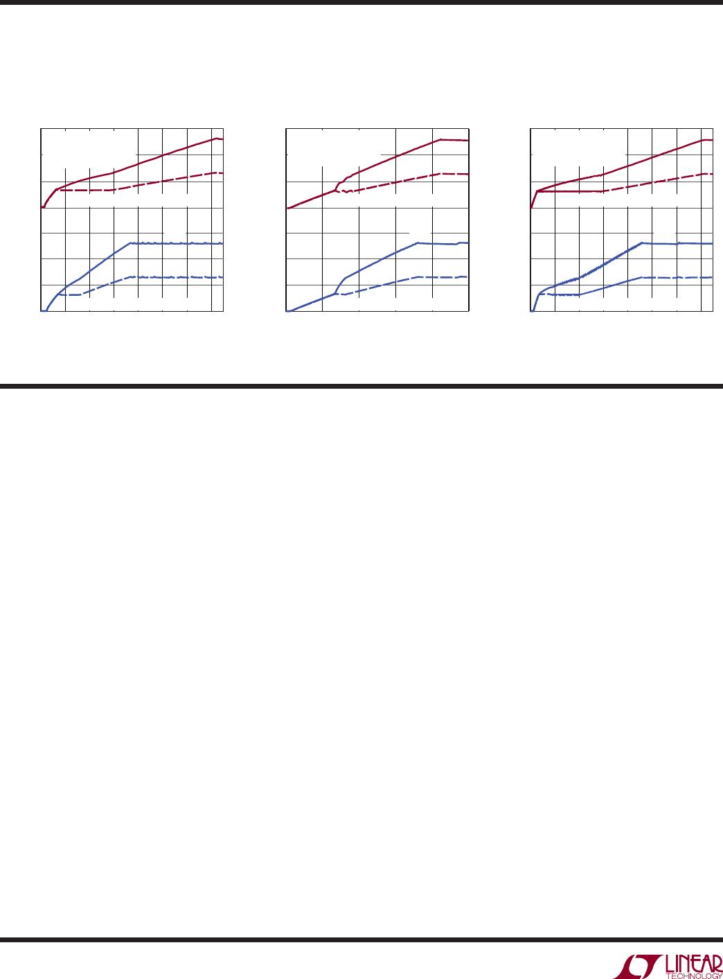
TIME (SECONDS)
0
SINGLE INDUCTOR
VOLTAGE (V)
DUAL INDUCTOR
VOLTAGE (V)
0
2
4
120
3625 G16
6
4
20 40 60 80 100 140
2
0
6
V
OUT
V
MID
V
MID
V
IN
= 3.6V, V
SEL
= 3.6V
R
PROG
= 143k
C
TOP
= C
BOT
= 10F
V
OUT
SINGLE INDUCTOR APPLICATION
DUAL INDUCTOR APPLICATION
TIME (SECONDS)
0
SINGLE INDUCTOR
VOLTAGE (V)
DUAL INDUCTOR
VOLTAGE (V)
0
2
4
200
3625 G17
6
4
50 100 150 250
2
0
6
V
OUT
V
MID
V
MID
V
IN
= 3.6V, V
SEL
= 3.6V
R
PROG
= 143k
C
TOP
= 10F, C
BOT
= 50F
V
OUT
SINGLE INDUCTOR APPLICATION
DUAL INDUCTOR APPLICATION
TIME (SECONDS)
0
SINGLE INDUCTOR
VOLTAGE (V)
DUAL INDUCTOR
VOLTAGE (V)
0
2
4
300
3625 G18
6
4
50 100 150 200 250 350
2
0
6
V
OUT
V
MID
V
MID
V
OUT
SINGLE INDUCTOR APPLICATION
DUAL INDUCTOR APPLICATION
V
IN
= 3.6V, V
SEL
= 3.6V
R
PROG
= 143k
C
TOP
= 50F, C
BOT
= 10F