19-2145; Rev 3; 10/12
For pricing, delivery, and ordering information, please contact Maxim Direct
at 1-888-629-4642, or visit Maxim’s website at www.maximintegrated.com.
MAX2900–MAX2904
200mW Single-Chip Transmitter ICs for
868MHz/915MHz ISM Bands
General Description
The MAX2900–MAX2904 complete single-chip 200mW
transmitters are designed for use in the 868MHz/
915MHz frequency bands. The MAX2900/MAX2901/
MAX2902 are compliant with the FCC CFR47 part 15.247
902MHz to 928MHz ISM-band specifications. MAX2903/
MAX2904 are compliant with the ETSI EN330-220 speci-
fication for the European 868MHz ISM band.
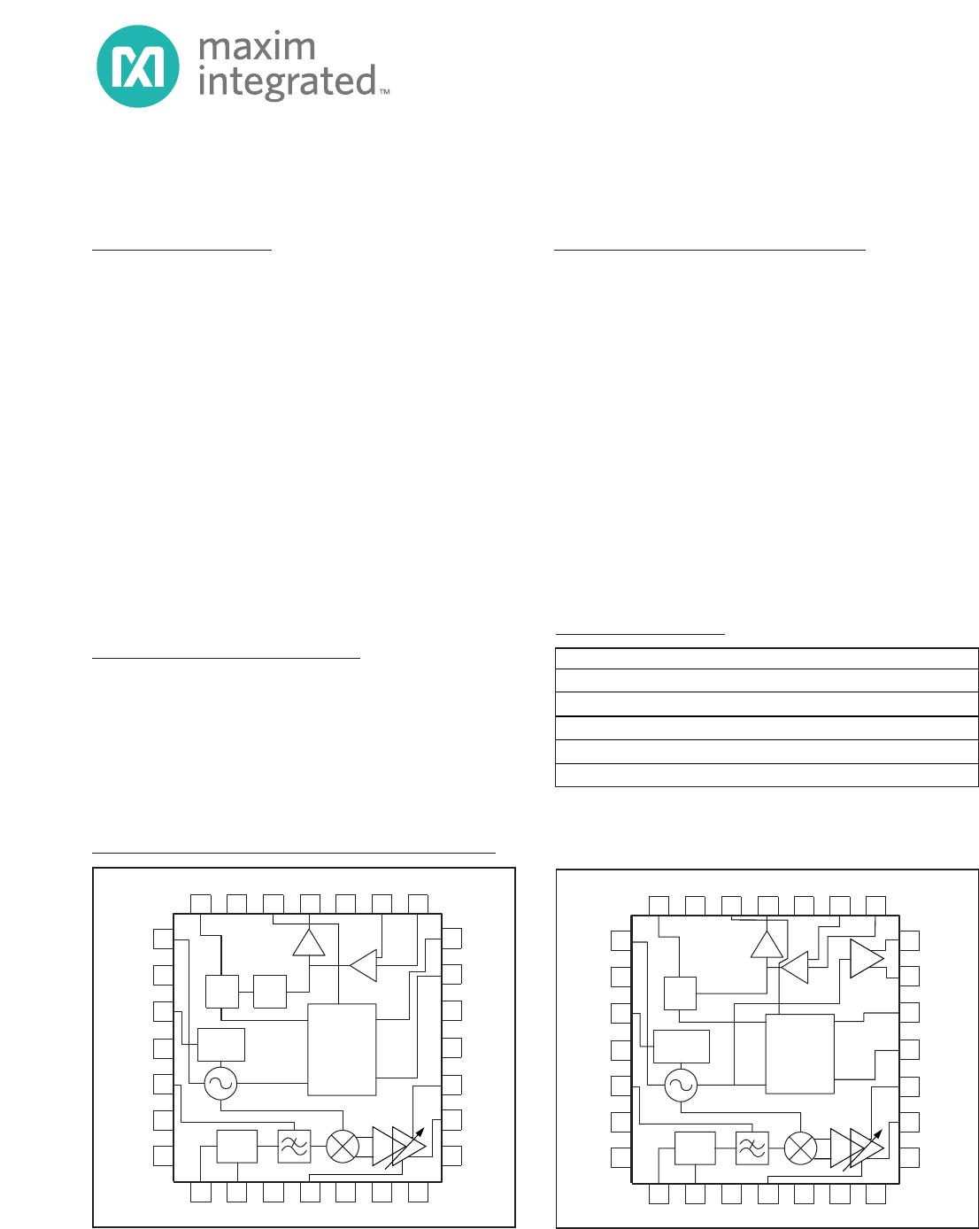
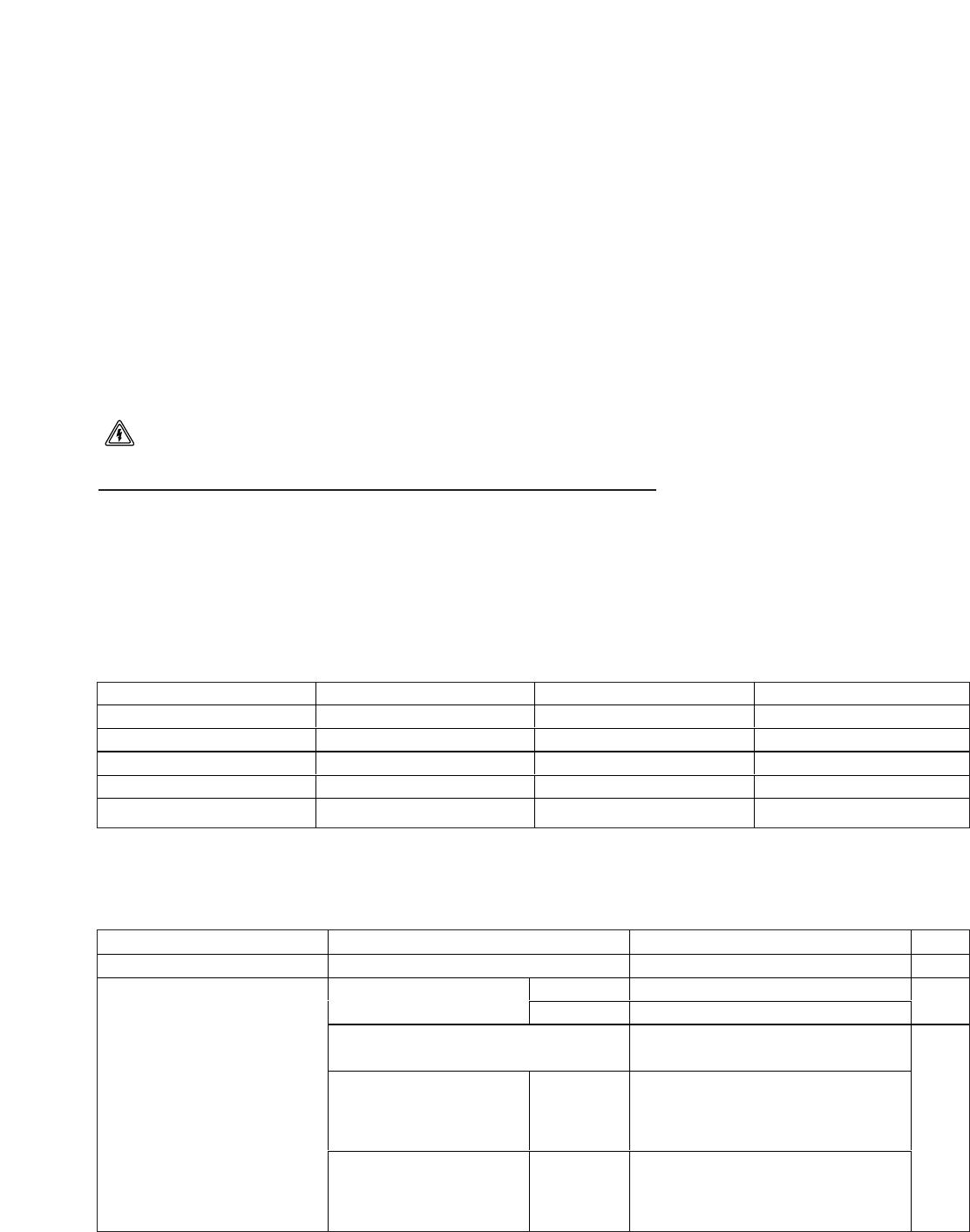
These transmitter ICs offer a high level of integration
while minimizing the number of external components.
This is achieved by full integration of the transmit modu-
lator, power amplifier, RF VCO, 8-channel frequency syn-
thesizer, and baseband PN sequence lowpass filter. By
filtering the BPSK modulation, the spurious emissions are
reduced, enabling up to eight independent transmit
channels in the U.S. ISM band. Inputs are provided for
spread-spectrum BPSK, ASK, and OOK. FM can be
achieved by directly modulating the VCO. The devices
are intended primarily for use with an external differential
antenna.
Applications
Automatic Meter Reading
Wireless Security Systems/Alarms
Wireless Sensors
Wireless Data Networks
Wireless Building Control
Features
o Versions for U.S. 902MHz to 928MHz Band and
European 868MHz Band
o -7dBm to +23dBm Adjustable Differential RF
Output Power
o +23dBm Output Power at 4.5V, +20dBm Output
Power at 3.0V
o Support BPSK, OOK, ASK, and FM Modulations
o Modulation Filter for Direct Sequence BPSK up to
8Mchips/s
o Fully Integrated VCO with On-Chip Tank
o Extremely Low Frequency Pulling for OOK
Modulation (typ 60kHz peak, 5kHz RMS)
o Integrated Frequency Synthesizer for up to
8 Channels (MAX2900)
o +2.7V to +4.5V Supply Operation
o Small 28-Pin QFN Package with Exposed Pad
(5mm
5mm)
1
3
2
4
5
6
7
21
19
20
18
17
16
15
810911121314
28
26
27 25 24 23 22
REFEN
EN
RLPF
VCC1
VREG
GND
VTUNE
GND
RF-
RF+
GND
DIVOUT
VCO-
VCO+
OSC
REFIN
VCC4
REFOUT
DIV63
VCC5
CPOUT
VCC3
PWRSET
LD
VASK
VCC2
OOKIN
MODIN
DUAL-
CHANNEL
(/62 OR /63)
SYNTHESIZER
CP
GATE
REG
MAX2901/
MAX2903
Functional Diagrams/Pin Configurations
Ordering Information
PART TEMP RANGE PIN-PACKAGE
MAX2900ETI+ -40°C to +85°C 28 QFN-EP*
MAX2901ETI+ -40°C to +85°C 28 QFN-EP*
MAX2902ETI+ -40°C to +85°C 28 QFN-EP*
MAX2903ETI+ -40°C to +85°C 28 QFN-EP*
MAX2904ETI+ -40°C to +85°C 28 QFN-EP*
Functional Diagrams/Pin Configurations are continued at end of data sheet.
1
3
2
4
5
6
7
21
19
20
18
17
16
15
810911121314
28
26
27 25 24 23 22
REFEN
EN
RLPF
VCC1
VREG
GND
VTUNE
GND
RF-
RF+
N.C.
N.C.
D1
D0
OSC
REFIN
VCC4
REFOUT
D2
VCC5
CPOUT
VCC3
PWRSET
LD
VASK
VCC2
OOKIN
MODIN
8-CHANNEL
SYNTHESIZER
CP
GATE
REG
÷4
MAX2900
+
Denotes a lead(Pb)-free/RoHS-compliant package.
*
Exposed pad
MAX2900–MAX2904
200mW Single-Chip Transmitter ICs for
868MHz/915MHz ISM Bands
2
Maxim Integrated
ABSOLUTE MAXIMUM RATINGS
DC ELECTRICAL CHARACTERISTICS
(V
CC
= +2.7V to +4.5V, EN = OOKIN = REFEN = high, T
A
= -40°C to +85°C. Typical values are at V
CC
= +4.5V, T
A
= +25°C, unless
otherwise noted.) (Note 1)
Stresses beyond those listed under “Absolute Maximum Ratings” may cause permanent damage to the device. These are stress ratings only, and functional
operation of the device at these or any other conditions beyond those indicated in the operational sections of the specifications is not implied. Exposure to
absolute maximum rating conditions for extended periods may affect device reliability.
V
CC
to GND...........................................................-0.3V to +5.0V
Analog/Digital Input Voltage to GND..........-0.3V to (V
CC
+ 0.3V)
Analog/Digital Input Current ..............................................±10µA
Continuous Power Dissipation (T
A
= +70°C)
28-Pin QFN-EP (derate 28.5mW/°C above +70°C)............2W
Operating Temperature Range ...........................-40°C to +85°C
Junction Temperature .....................................................+150°C
Storage Temperature Range .............................-65°C to +150°C
Lead Temperature (soldering, 10s) .................................+300°C
PARAMETER CONDITIONS MIN -3σ TYP +3σ MAX UNITS
Supply Voltage 2.7 4.5 4.5 V
V
CC
= +4.0V 0.7 10
Shutdown mode: EN =
REFEN = low
V
CC
= +4.5V 60 200
µA
Synth mode: OOKIN = low
(MAX2900/MAX2901/MAX2903 only)
32 40
Transmit mode with output
matching optimized for
+23dBm at +4.5V: PWRSET
loaded with 22kΩ resistor
T
A
= -40°C
to +85°C
150 200
Supply Current
Transmit mode with output
matching optimized for
+20dBm at +3.0V: PWRSET
loaded with 22kΩ resistor
T
A
= -40°C
to +85°C
110 135
mA
Five different versions are available. The versions differ
by their frequency band of operation, and by the synthe-
sizer’s mode of operation. The MAX2900 has an internal
8-channel synthesizer.
The MAX2901 and MAX2903 are dual-channel versions
with a selectable internal synthesizer division ratio of 62
or 63. The MAX2901 operates in the 902MHz to
928MHz ISM band and the MAX2903 operates in the
867MHz to 870MHz European ISM band.
The MAX2902 and MAX2904 require an off-chip fre-
quency synthesizer. The MAX2902 operates in the
902MHz– 928MHz ISM band and MAX2904 operates in
the 867MHz–870MHz European ISM band.
The MAX2901–MAX2904 provide LO outputs to drive a
receiver and/or an external synthesizer.
PART FREQUENCY RANGE (MHz) SYNTHESIZER LO OUTPUTS
MAX2900ETI+ 902 to 928 Internal 8 selectable channels No
MAX2901ETI+ 902 to 928 Internal 2 selectable channels Yes
MAX2902ETI+ 902 to 928 Off-chip Yes
MAX2903ETI+ 867 to 870 Internal 2 selectable channels Yes
MAX2904ETI+ 867 to 870 Off-chip Yes
Part Selection Information
CAUTION! ESD SENSITIVE DEVICE
MAX2900–MAX2904
200mW Single-Chip Transmitter ICs for
868MHz/915MHz ISM Bands
3
Maxim Integrated
DC ELECTRICAL CHARACTERISTICS (continued)
(V
CC
= +2.7V to +4.5V, EN = OOKIN = REFEN = high, T
A
= -40°C to +85°C. Typical values are at V
CC
= +4.5V, T
A
= +25°C, unless
otherwise noted.) (Note 1)
PARAMETER CONDITIONS MIN -3σ TYP +3σ MAX UNITS
Transmit mode with output
matching optimized for
+17dBm at +3.0V: PWRSET
loaded with 36kΩ resistor
T
A
= +25°C 75
Transmit mode with output
matching optimized for
+14dBm at +3.0V: PWRSET
loaded with 51kΩ resistor
T
A
= +25°C 57
Reference-only mode: EN = low 2 3
Supply Current (continued)
PA standby mode: OOKIN = low
(MAX2902/MAX2904 only)
29 33
mA
VCO Input Tuning Pin Current VTUNE = +4.5V, T
A
= +25°C 0.02 2 µA
VREG VCO Regulator Voltage 2.0 V
D IG IT A L IN PU T /O U T PU T S ( P IN S E N , RE FE N , D 0, D 1, D 2, M O D IN , O OKIN , LD )
Input Level High
V
CC
- 0.5V
V
Input Level Low 0.5 V
Input Bias Current -10 10 µA
Output Level High
V
CC
- 0.4
V
Output Level Low 0.4 V
Output Current -100 100 µA
ANALOG CONTROL INPUTS (PINS PWRSET, RLPF, VASK)
PWRSET Voltage 1.2 V
RLPF Voltage 1.2 V
VASK Input Impedance 100 220 400 kΩ

MAX2903ETI+T

Mfr. #:
Manufacturer:
Maxim Integrated
Description:
RF Transmitter 200mW Sngl-Chip Txr 868/915MHz ISM Bands
Lifecycle:
New from this manufacturer.
Delivery:
DHL FedEx Ups TNT EMS
Payment:
T/T Paypal Visa MoneyGram Western Union