MAX2900–MAX2904
200mW Single-Chip Transmitter ICs for
868MHz/915MHz ISM Bands
7
Maxim Integrated
Typical Operating Characteristics (continued)
(MAX290_ EV kits. V
CC
= +4.5V, f
RF
= 917.28MHz (MAX2900/MAX2901/MAX2902) or f
RF
= 868MHz (MAX2903/MAX2904), R
RLPF
=
68kΩ, R
PWRSET
= 22kΩ, VASK = VREG, f
REF
= 14.56MHz (MAX2900/MAX2901/MAX2902) or f
REF
= 13.78MHz (MAX2903/MAX2904),
chip rate on MODIN = 1.22 Mbps, RF output matching network optimized for +23dBm, V
CC
= 4.5V, T
A
= +25°C, unless
otherwise noted.)
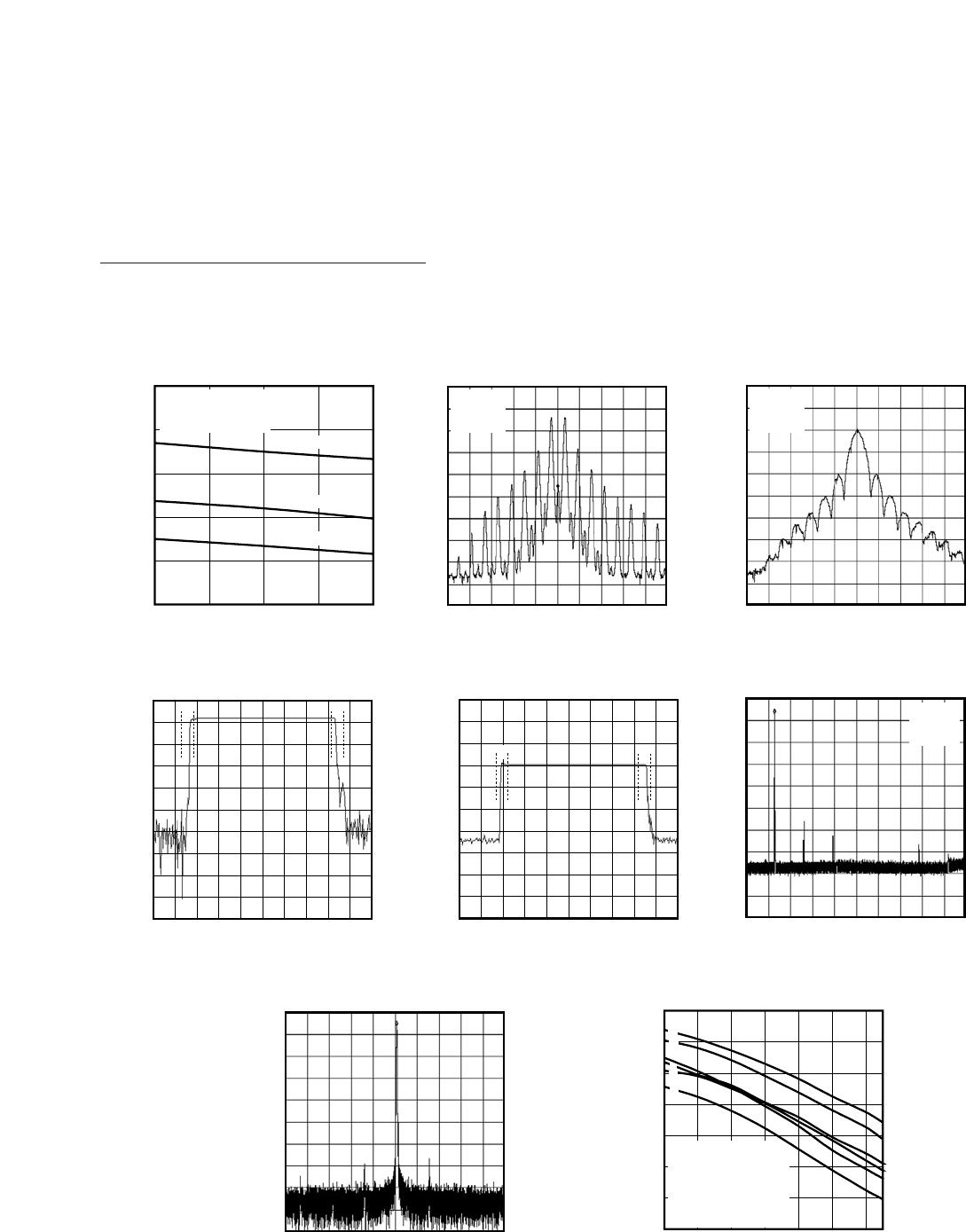
RF POWER vs. FREQUENCY
(MAX2903/MAX2904)
MAX2900 toc10
FREQUENCY (MHz)
RF POWER (dBm)
872868864
13
14
15
16
17
12
860 876
V
CC
= +3.6V
V
CC
= +3.0V
V
CC
= +2.7V
RF OUTPUT MATCHING
OPTIMIZED FOR +14dBm
OUTPUT AT V
CC
= +3.0V
OUTPUT SPECTRUM WITH 600kHz
SQUARE WAVE INPUT AT MODIN
MAX2900 toc11
30dBm
-70dBm
10dB/div
MKR
917.31MHz
-16.33dBm
CENTER 917.28MHz
SPAN 20MHz
OUTPUT SPECTRUM WITH PN SEQUENCE
AT 1.22MHz AT MODIN
MAX2900 toc12
30dBm
-70dBm
10dB/div
MKR
917.35MHz
8.17dBm
CENTER 917.28MHz
SPAN 20MHz
RF OUT RISE AND FALL TIME TRANSIENT
WITH SQUARE OOK
MAX2900 toc13
0dBVp-p
-100dBVp-p
10dB/div
T
r
T
f
START 46
μ
s
STOP 86
μ
s
RF OUT RISE AND FALL TIME TRANSIENT
WITH SQUARE ASK
MAX2900 toc14
22dBVp-p
-78dBVp-p
10dB/div
T
r
T
f
START 45
μ
s
STOP 85
μ
s
SPURIOUS LEVEL FROM
DC TO 7TH HARMONIC
MAX2900 toc15
MKR
910MHz
23.17dBm
30dBm
-70dBm
10dB/div
START 0Hz
STOP 7GHz
SPURIOUS LEVEL BETWEEN ±50MHz
FROM CARRIER FREQUENCY
MAX2900 toc16
30dBm
-70dBm
10dB/div
CENTER 917.28MHz
SPAN 100MHz
TRANSMITTER EFFICIENCY vs. R
PWRSET
MAX2900 toc17
R
PWRSET
(kΩ)
TRANSMITTER EFFICIENCY (%)
383430262218
15
20
25
30
35
40
45
10
14
A
B
C
E
F
D
A: V
CC
= 4.5V, T
A
= -40
°
C
B: V
CC
= 4.5V, T
A
= +25°C
C: V
CC
= 4.5V, T
A
= +85°C
D: V
CC
= 2.7V, T
A
= -40°C
E: V
CC
= 2.7V, T
A
= +25°C
F: V
CC
= 2.7V, T
A
= +85°C
MAX2900–MAX2904
200mW Single-Chip Transmitter ICs for
868MHz/915MHz ISM Bands
8
Maxim Integrated
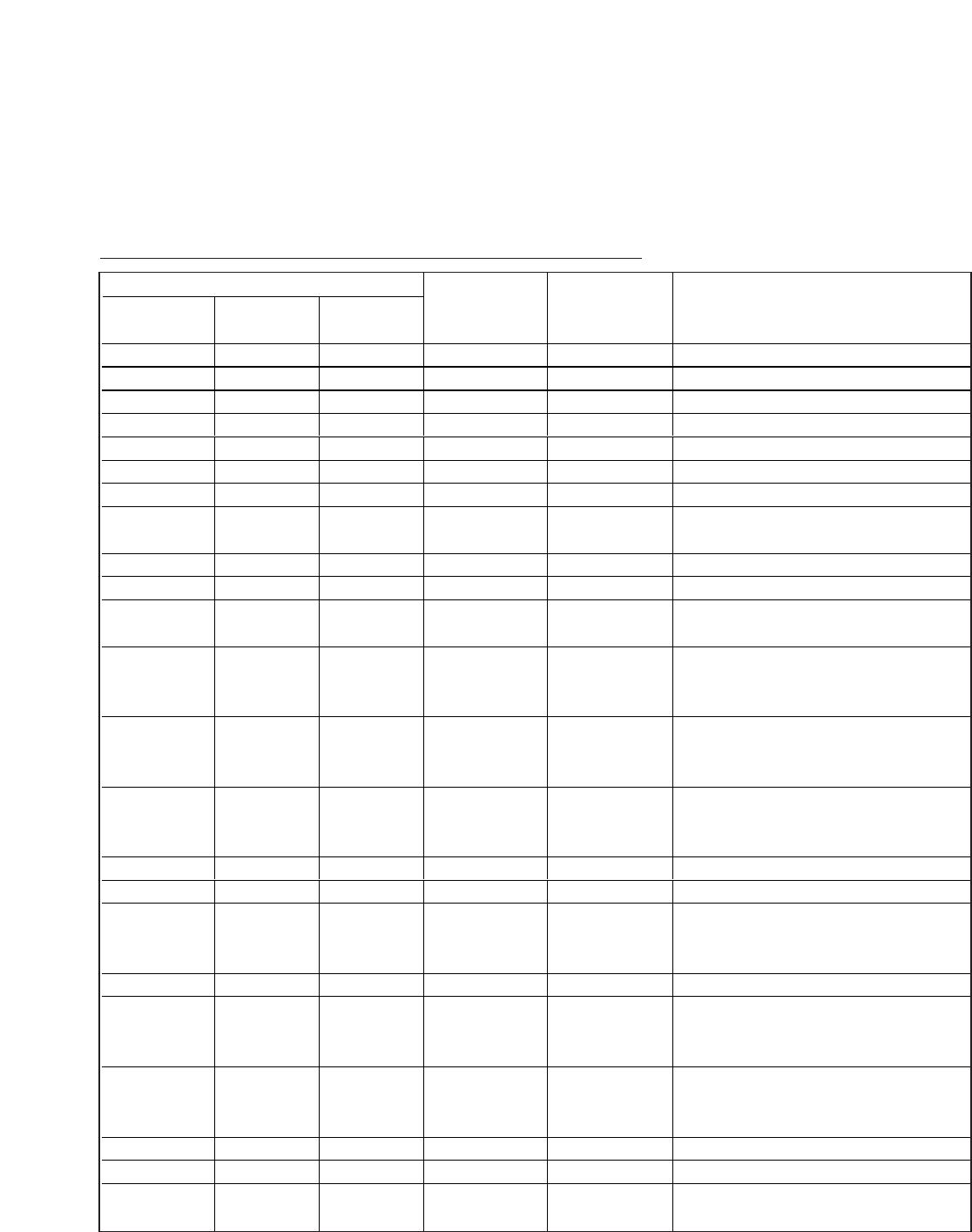
Pin Description
PIN
MAX2900
MAX2901
MAX2903
MAX2902
MAX2904
NAME PIN TYPE FUNCTION
1 1 1 VTUNE Analog Input VCO tuning voltage input
2 2 2 GND Supply Pin Ground
3 3 3 VREG
Analog
Input/Output
Regulated voltage output to supply the VCO.
Bypass with a 0.01µF capacitor to GND as
close to the part as possible.
4 4 4 VCC1 Supply Pin
Power supply pin for VCO circuits. Bypass
with a 1000pF and a 10µF capacitor to GND
as close to the part as possible.
5 5 5 RLPF
Analog Input
Resistor to Ground
Resistor to ground on this pin sets the
modulation filter bandwidth.
6 6 6 EN Digital Input
Chip-enable digital input pin. Set EN low
maintain the chip in power-down mode.
7 7 7 REFEN Digital Input
Enable for crystal oscillator and frequency
reference buffer.
8 8 8 MODIN Digital Input BPSK modulation input
9 9 9 OOKIN Digital Input On-off keying modulation. On state = high.
10 10 10 VCC2 Supply
Power supply pin for internal RF buffer
circuits. Bypass with a 100pF and a 0.01µF
capacitor to GND as close to the part as
possible.
11 11 11 VASK
Analog Voltage
Input
ASK voltage input pin
12 12 LD Digital Output
Lock detector output digital pin. Level is
high when PLL is inside lock range.
12 D.C. Do NOT Connect
13 13 13 PWRSET
Anal og Inp ut
Resi stor to Gr ound
Current input set to adjust output power.
14 14 14 VCC3 Supply
P ow er sup p l y p i n for RF p ow er am p l i fi er
ci r cui ts. Byp ass w i th a 100p F cap aci tor to GN D
as cl ose to the p ar t as p ossi b l e.
MAX2900–MAX2904
200mW Single-Chip Transmitter ICs for
868MHz/915MHz ISM Bands
9
Maxim Integrated
Pin Description (continued)
PIN
MAX2900
MAX2901
MAX2903
MAX2902
MAX2904
NAME PIN TYPE FUNCTION
15 15 15 GND Supply Pin Ground
16, 17 16, 17 16, 17 RF-, RF+ RF Output RF d i ffer enti al outp ut, op en- col l ector typ e
18 N.C. Not Connected
18 GND Supply Pin Ground
18 D.C. Do Not Connect
19 19 N.C. Not Connected
19 DIVOUT ECL Output Divider output
20, 21 20, 21 VCO-, VCO+
Open Collector
RF
VCO output (differential)
20 D1 Digital Input Channel selection bit 1
21 D0 Digital Input Channel selection bit 0
22 22 22 OSC Analog Input
Crystal oscillator connection. See Typical
Operating Circuit.
23 23 23 REFIN
Analog Voltage
Input
Refer ence i np ut p i n anal og ( can b e used as
i np ut or as cr ystal osci l l ator d r i ver ) . See
Typical Operating Circuit.
24 24 VCC4 Supply Pin
Power-supply pin for the synthesizer circuits.
Bypass with a 1000pF capacitor to GND as
close to the part as possible.
24 VCC4 Supply Pin
Power-supply pin for the digital circuits.
Bypass with a 100pF capacitor to GND as
close to the part as possible.
25 25 25 REFOUT Analog Output Buffered clock analog output pin
26 D2 Digital Input Channel selection bit 2
26 DIV63 Digital Input
Division ratio selections (division ratio = 62
when DIV63 = high; division
ratio = 63 when DIV63 = low).
26 N.C. Not Connected
27 27 VCC5 Supply Pin
Power-supply pin for charge pump circuits.
Bypass with a 100pF capacitor to GND as
close to the part as possible.
27 VCC5 Supply Pin
Power-supply pin. Bypass with a 100pF
capacitor to GND as close to the part as
possible.
28 28 CPOUT Analog Output Charge pump output pin
28 D.C. Do Not Connect
GROUND GROUND GROUND GROUND
Electrical
Ground
Back side of package is connected to
ground.
MAX2903ETI+T

Mfr. #:
Manufacturer:
Maxim Integrated
Description:
RF Transmitter 200mW Sngl-Chip Txr 868/915MHz ISM Bands
Lifecycle:
New from this manufacturer.
Delivery:
DHL FedEx Ups TNT EMS
Payment:
T/T Paypal Visa MoneyGram Western Union