MAX2900–MAX2904
200mW Single-Chip Transmitter ICs for
868MHz/915MHz ISM Bands
10
Maxim Integrated
Detailed Description
Principles of Operation
When EN goes high, the reference and the VCO start
while the PA stays in the off mode. For MAX2900/
MAX2901/MAX2903, the PLL also starts when EN goes
high. After the lock-detect pin LD goes high, the PA is set
to stand-by mode. For the MAX2902/MAX2904, the VCO
loop has to be closed by using an external synthesizer.
After this, pulling OOKIN high turns on the PA. The inter-
nal modulation filter smoothes the power ramp-up of the
PA.
The modulation filter BW is typically 0.8MHz, used for a
1.22Mbps chip rate, and can be adjusted by varying
RLPF. A high value can be used for RLPF to get a slow
PA ramping up when BPSK is not used.
The reference blocks can be turned on separately (and
earlier) by pulling REFEN high, to allow the crystal fre-
quency to settle.
The device supports various modulation modes:
• BPSK, filtered by the internal modulation filter, is
obtained through the MODIN pin. This is the pre-
ferred mode of operation for MAX2900.
• OOK is obtained digitally with the OOKIN pin.
• ASK is obtained through the ASK pin.
• FM is imposed on the VCO or the reference.
• FM is the preferred mode of operation for the
MAX2903/MAX2904 due to the narrowband opera-
tion common in Europe.
The maximum output power is set by the output match-
ing network and the external biasing resistor on the
PWRSET pin.
For the MAX2901–MAX2904, differential LO outputs are
provided to drive a companion receiver and/or an
external synthesizer.
Power-Up Modes
The circuit has four modes of operations, defined as
follows:
1) Shutdown mode: Pin EN and REFEN are low, all
functions are off, and the current consumption is
leakage only.
2) Synth mode: Pin EN and REFEN are high, pin
OOKIN is low. The reference circuits, VCO, and
synthesizer are turned on. The power amplifier is in
stand-by mode. Total current is less than 50mA.
Note that as long as the LD pin is not going high,
indicating that the PLL is unlocked, OOKIN high is
ignored.
3) Transmit mode: Pin EN and REFEN are high. If output
pin LD is high, the device is ready to transmit. When
OOKIN is high, the power amplifier is turned on. The
current consumption varies between 50mA and
120mA, depending on the output power requested by
the combination of the OOK duty cycle, the PWRSET
value, and output matching circuit.
4) Reference Only mode: This mode enables the use
of the crystal reference from the IC to drive the
external logic ICs. To obtain this mode, set the
REFEN pin high and EN low. In this mode, only the
reference circuit turns on, the crystal oscillator starts,
and the clock is present at the REFOUT pin. The cur-
rent consumption remains much lower than that in the
SYNTH mode because the VCO, synthesizer, and PA
standby circuits are off. When EN goes high, the IC
goes into the SYNTH mode.
Synthesizer Programming
The three pins D0–D2 (MAX2900) and DIV63 (MAX2901/
MAX2903) are used as digital entries to program the syn-
thesizer division ratios. Tables 4 and 5 show the division
ratios obtained for the various pin logic levels.
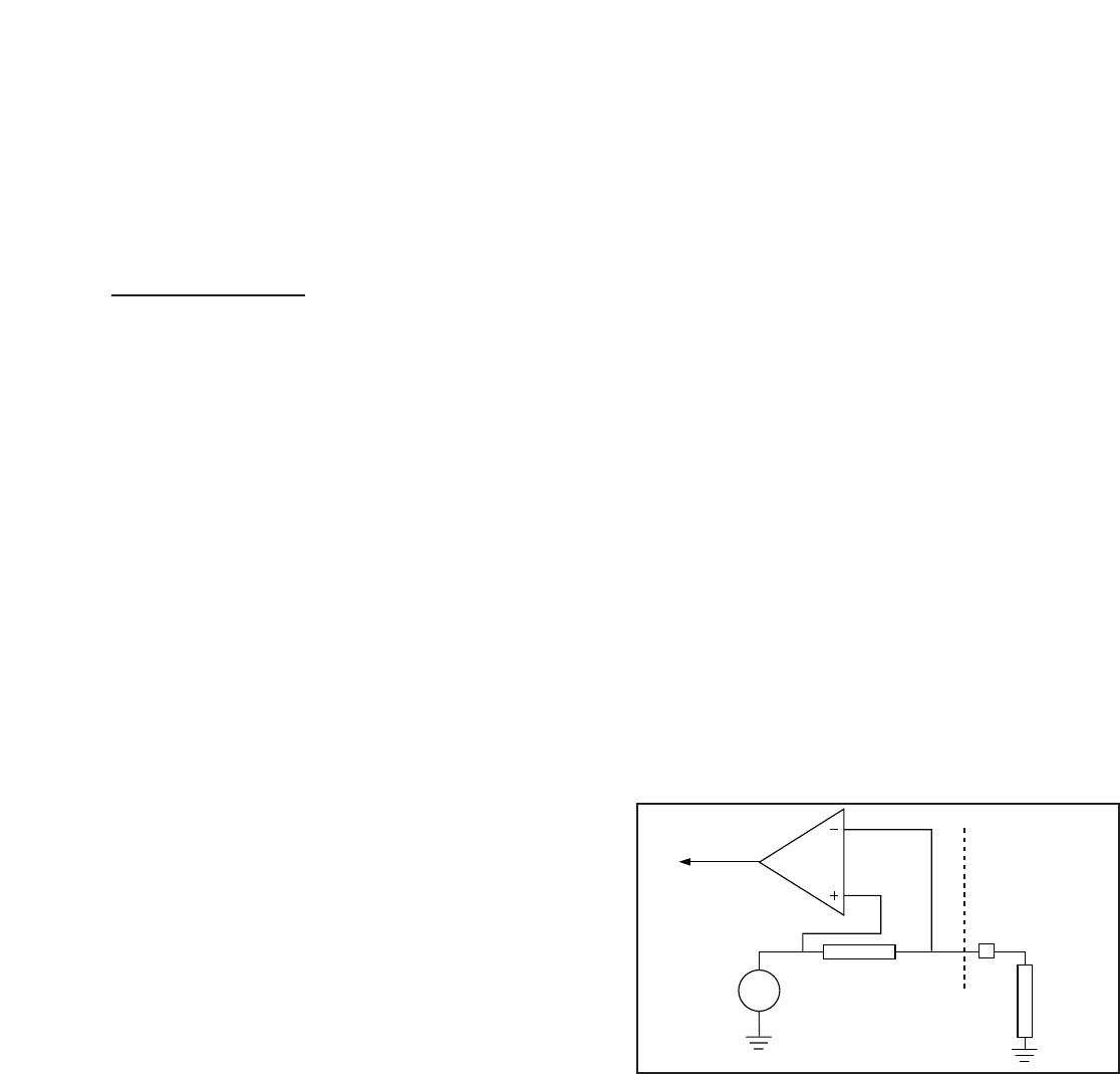
Analog Input Control Pins
The two pins PWRSET and VASK are analog inputs
used to control the power of the transmitter. The equiv-
alent input schematics are defined in Figures 1, 2, and
3. The PWRSET pin sets the biasing of the amplification
chain. Because the last stage of the amplifier operates
in saturation, the output power mostly depends on the
load and supply voltage. The purpose of the PWRSET
resistor is to achieve optimum biasing (and therefore
efficiency) for various maximum output power configu-
rations. For a given application with a known operating
voltage and peak power, a fixed value of resistor is
determined. The output power range of -7dBm to
+23dBm at 4.5V is obtained by choosing a combination
of output load line and the resistor on PWRSET; 22kΩ is