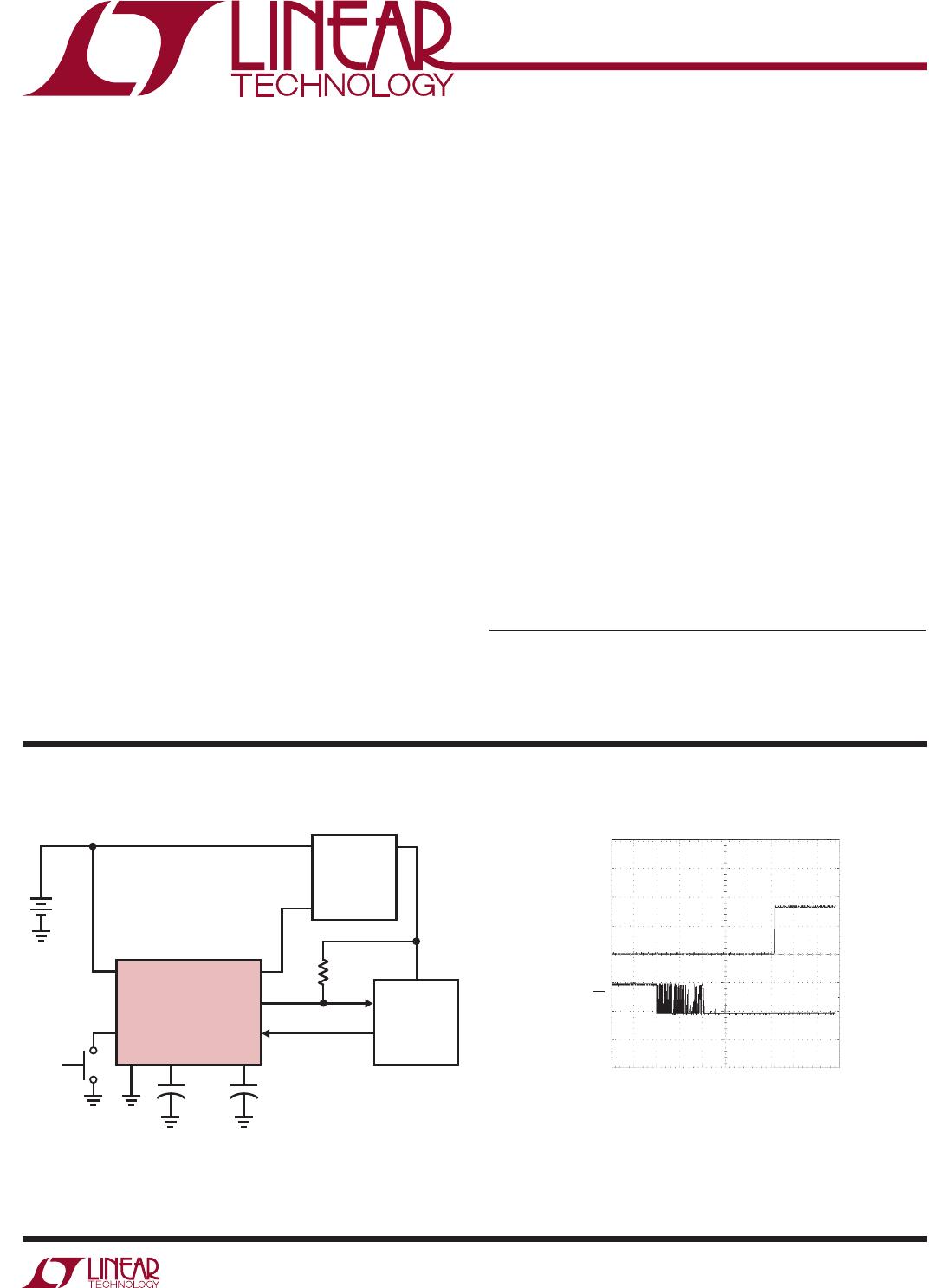
LTC2950-1/LTC2950-2
3
295012fd
SYMBOL PARAMETER CONDITIONS MIN TYP MAX UNITS
V
IN
Supply Voltage Range Steady State Operation
l
2.7 26.4 V
I
IN
V
IN
Supply Current System Power On, V
IN
= 2.7V to 24V
l
6 12 µA
V
UVL
V
IN
Undervoltage Lockout V
IN
Falling
l
2.2 2.3 2.4 V
V
UVL(HYST)
V
IN
Undervoltage Lockout
Hysteresis
50 300 600 mV
Pushbutton, Enable (PB, EN/EN)
V
PB(MIN, MAX)
PB Voltage Range Single-Ended
l
–1 26.4 V
I
PB
PB Input Current 2.5V < V
PB
< 26.4V
V
PB
= 1V
V
PB
= 0.6V
l
l
l
–1
–3
–6
–9
±1
–12
–15
µA
µA
µA
V
PB(VTH)
PB Input Threshold PB Falling
l
0.6 0.8 1 V
V
PB(VOC)
PB Open Circuit Voltage I
PB
= –1µA 1 1.6 2 V
t
EN/EN, Lock Out
EN/EN Lock Out Time (Note 5)
Enable Released → Enable Asserted
l
200 256 325 ms
I
EN/EN(LKG)
EN/EN Leakage Current V
EN/
EN
= 1V, Sink Current Off
l
±0.1 µA
V
EN/EN(VOL)
EN/EN Voltage Output Low I
EN/
EN
= 3mA
l
0.11 0.4 V
Debounce Timing Pins (ONT, OFFT)
I
ONT, OFFT(PU)
ONT/OFFT Pull Up Current V
ONT, OFFT
= 0V
l
–2.4 –3 –3.6 µA
I
ONT, OFFT(PD)
ONT/OFFT Pull Down Current V
ONT, OFFT
= 1.3V
l
2.4 3 3.6 µA
t
DB, On
Internal Turn On Debounce Time
ONT Pin Float, PB Falling → Enable Asserted
l
26 32 41 ms
t
ONT
Additional Adjustable Turn On Time C
ONT
= 1500pF
l
9 11.5 13.5 ms
t
DB, Off
Internal Turn Off Debounce Time
OFFT Pin Float, PB Falling → INT Falling
l
26 32 41 ms
t
OFFT
Additional Adjustable Turn Off Time C
OFFT
= 1500pF
l
9 11.5 13.5 ms
µP Handshake Pins (INT, KILL)
I
INT(LKG)
INT Leakage Current V
INT
= 3V
l
±1 µA
V
INT(VOL)
INT Output Voltage Low I
INT
= 3mA
l
0.11 0.4 V
V
KILL(TH)
KILL Input Threshold Voltage KILL Falling
l
0.57 0.6 0.63 V
V
KILL(HYST)
KILL Input Threshold Hysteresis 10 30 50 mV
I
KILL(LKG)
KILL Leakage Current V
KILL
= 0.6V ±0.1 µA
t
KILL(PW)
KILL Minimum Pulse Width
l
30 µs
t
KILL(PD)
KILL Propagation Delay
KILL Falling → Enable Released
l
30 µs
t
KILL, On Blank
KILL Turn On Blanking (Note 3)
KILL = Low, Enable Asserted → Enable Released
l
400 512 650 ms
t
KILL, Off Delay
KILL Turn Off Delay (Note 4)
KILL = High, INT Asserted → Enable Released
l
800 1024 1300 ms
Note 1: Stresses beyond those listed under Absolute Maximum Ratings
may cause permanent damage to the device. Exposure to any Absolute
Maximum Rating condition for extended periods may affect device
reliability and lifetime.
Note 2: All currents into pins are positive; all voltages are referenced to
GND unless otherwise noted.
Note 3: The KILL turn on blanking timer period is the waiting period
immediately after the enable output is asserted. This blanking time allows
sufficient time for the DC/DC converter and the µP to perform power up
tasks. The KILL and PB inputs are ignored during this period. If KILL remains
low at the end of this time period, the enable output is released, thus turning
off system power. This time delay does not include t
DB, ON
or t
ONT
.
Note 4: The KILL turn off delay is the maximum delay from the initiation
of a shutdown sequence (INT falling), to the release of the enable output.
If the KILL input switches low at any time during this period, enable is
released, thus turning off system power. This time is internally fixed at
1024ms. This time delay does not include t
DB, OFF
or t
OFFT
.
Note 5: The enable lock out time is designed to allow an application to
properly power down such that the next power up sequence starts from a
consistent powered down configuration. PB
is ignored during this lock out
time. This time delay does not include t
DB, ON
or t
ONT
.
elecTrical characTerisTics
The l denotes the specifications which apply over the full operating
temperature range, otherwise specifications are at T
A
= 25°C. V
IN
= 2.7V to 26.4V, unless otherwise noted. (Note 2)