LTC2950-1/LTC2950-2
13
295012fd
below 0.6V, then an appropriate bypass capacitor should
be connected to the KILL pin.
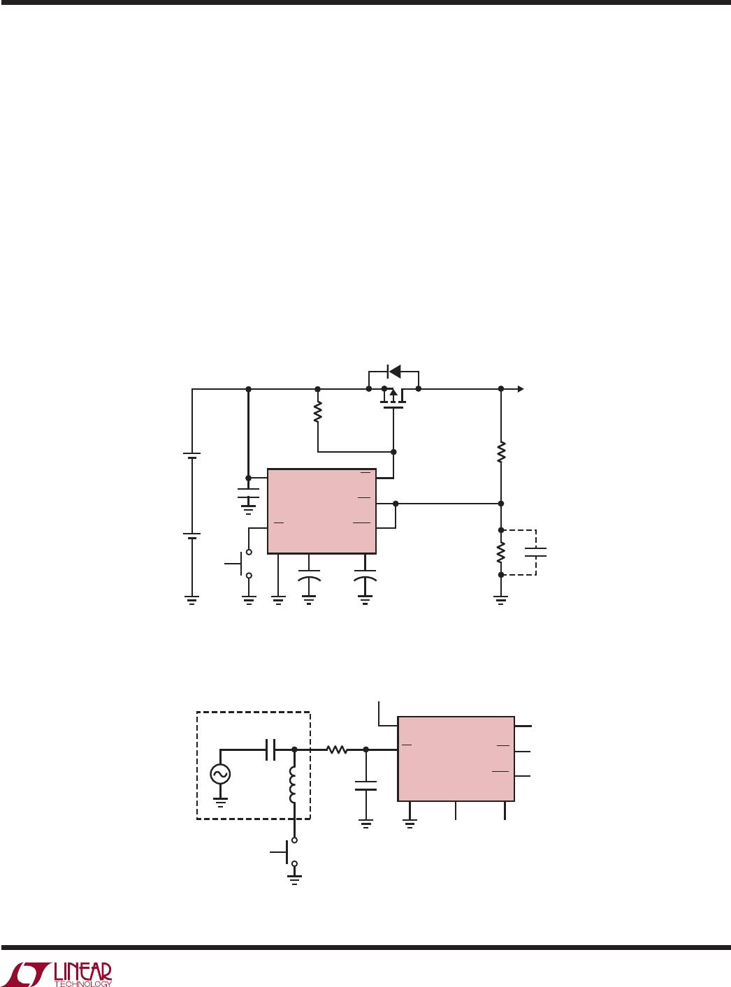
PowerPath™ Switching
The EN open drain output of the LTC2950-2 is designed to
switch on/off an external power PFET. This allows a user
to connect/disconnect a power supply (or battery) to its
load by toggling the PB pin. Figure 7 shows the LTC2950-2
controlling a two cell Li-Ion battery application. The INT
and KILL pins are connected to the output of the PFET
through a resistor divider. The KILL pin serves as a voltage
monitor. When V
OUT
drops below 6V, the EN pin is open
circuited 30µs later.
V
OUT
R1
909k
1%
R4
100k
1%
C3*
0.1µF
2950 F07
C4
0.1µF
CERAMIC
*OPTIONAL
OPEN DRAIN OUTPUT
V
TH
= 0.6V INPUT
R5
100K
M1
+
4.2V
SINGLE CELL
Li-Ion BATTERY
+
4.2V
SINGLE CELL
Li-Ion BATTERY
OPTIONAL GLITCH
FILTER CAPACITOR
V
OUT
,TRIP POINT = 6V
PB
EN
INT
KILL
LTC2950-2
GND ONT OFFT
V
IN
C
ONT
*
0.033µF
C
OFFT
*
0.033µF
PB
V
IN
LTC2950-1
GND ONT
R6
5k
2950 F08
TRACE
CAPACITANCE
PARASITICS
C5
0.1µF
DETAILS OMITTED
FOR CLARITY
TRACE
INDUCTANCE
NOISE
EN
INT
KILL
OFFT
V
IN
Figure 7. PowerPath Control with 6V Undervoltage Detect
Figure 8. Noisy PB Trace
PB Pin in a Noisy Environment
The rugged PB pin is designed to operate in noisy envi-
ronments. Transients below ground (>–6V) and above V
IN
(<30V) will not damage the rugged PB pin. Additionally,
the PB pin can withstand ESD HBM strikes up to ±10kV.
In order to keep external noise from coupling inside the
LTC2950, place an R-C network close to the PB pin. A 5k
resistor and a 0.1µF capacitor should suffice for most
noisy applications (see Figure 8).
External Pull-Up Resistor on PB
An internal pull-up resistor on the PB pin makes an ex-
ternal pull-up resistor unnecessary. Leakage current on
Typical applicaTions
LTC2950-1/LTC2950-2
14
295012fd
the PB board trace, however, will affect the open circuit
voltage on the PB pin. If the leakage is too large (>2µA),
the PB voltage may fall close to the threshold window. To
mitigate the effect of the board leakage, a 10k resistor to
V
IN
is recommended (see Figure 9).
PB
V
IN
LTC2950-1/
LTC2950-2
GND
EXTERNAL BOARD
LEAKAGE CURRENT
100k
2.4V
R7
10k
2950 F09
>2µA
PINS OMITTED
FOR CLARITY
IF EXTERNAL PARASITIC BOARD
LEAKAGE >2µA, USE EXTERNAL
PULL-UP RESISTOR
V
IN
Figure 9. External Pull-Up Resistor on PB Pin
Reverse Battery Protection
To protect the LTC2950 from a reverse battery connection,
place a 1k resistor in series with the V
IN
pin (see Figure 10).
Typical applicaTions
LTC2950-1/LTC2950-2
15
295012fd
package DescripTion
DDB Package
8-Lead Plastic DFN (3mm × 2mm)
(Reference LTC DWG # 05-08-1702 Rev B)
2.00 ±0.10
(2 SIDES)
NOTE:
1. DRAWING CONFORMS TO VERSION (WECD-1) IN JEDEC PACKAGE OUTLINE M0-229
2. DRAWING NOT TO SCALE
3. ALL DIMENSIONS ARE IN MILLIMETERS
4. DIMENSIONS OF EXPOSED PAD ON BOTTOM OF PACKAGE DO NOT INCLUDE
MOLD FLASH. MOLD FLASH, IF PRESENT, SHALL NOT EXCEED 0.15mm ON ANY SIDE
5. EXPOSED PAD SHALL BE SOLDER PLATED
6. SHADED AREA IS ONLY A REFERENCE FOR PIN 1 LOCATION ON THE TOP AND BOTTOM OF PACKAGE
0.40 ± 0.10
BOTTOM VIEW—EXPOSED PAD
0.56 ± 0.05
(2 SIDES)
0.75 ±0.05
R = 0.115
TYP
R = 0.05
TYP
2.15 ±0.05
(2 SIDES)
3.00 ±0.10
(2 SIDES)
14
85
PIN 1 BAR
TOP MARK
(SEE NOTE 6)
0.200 REF
0 – 0.05
(DDB8) DFN 0905 REV B
0.25 ± 0.05
2.20 ±0.05
(2 SIDES)
RECOMMENDED SOLDER PAD PITCH AND DIMENSIONS
0.61 ±0.05
(2 SIDES)
1.15 ±0.05
0.70 ±0.05
2.55 ±0.05
PACKAGE
OUTLINE
0.25 ± 0.05
0.50 BSC
PIN 1
R = 0.20 OR
0.25 × 45°
CHAMFER
0.50 BSC

LTC2950CDDB-2#TRMPBF

Mfr. #:
Manufacturer:
Analog Devices Inc.
Description:
Supervisory Circuits Basic Push Button On/Off Controller (Adjustbale On and Off Timers)
Lifecycle:
New from this manufacturer.
Delivery:
DHL FedEx Ups TNT EMS
Payment:
T/T Paypal Visa MoneyGram Western Union