LTC2950-1/LTC2950-2
9
295012fd
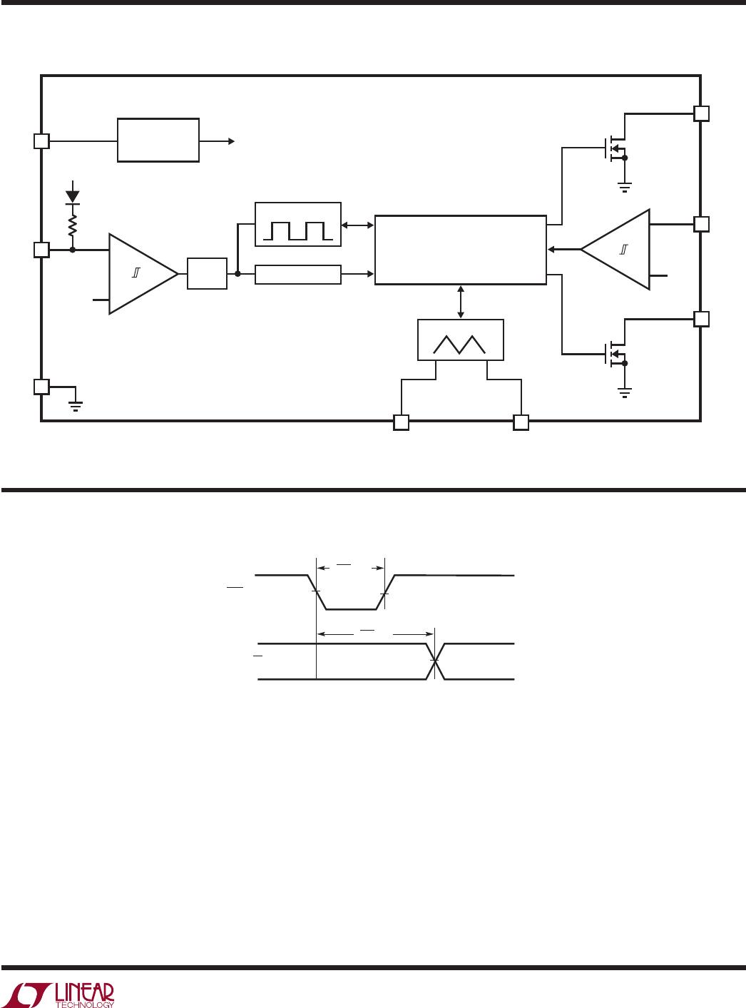
Description
The LTC2950 is a low power (6µA), wide input voltage
range (2.7V to 26.4V), pushbutton on/off controller that
can interface to a µP and a power supply. The turn-on and
turn-off debounce times are extendable using optional
external capacitors. A simple interface (INT output, KILL
input) allows a system to power on and power off in a
controlled manner.
Turn On
When power is first applied to the LTC2950, the part ini-
tializes the output pins. Any DC/DC converters connected
to the EN/EN pin will therefore be held off. To assert the
enable output, PB must be held low for a minimum of
32ms (t
DB, ON
). The LTC2950 provides additional turn on
debounce time via an optional capacitor connected to the
ONT pin (t
ONT
). The following equation describes the ad-
ditional time that PB must be held low before asserting
the enable output. C
ONT
is the ONT external capacitor:
C
ONT
= 1.56E-4 [µF/ms] • (t
ONT
– 1ms)
Once the enable output is asserted, any DC/DC converters
connected to this pin are turned on. The KILL input from
the µP is ignored during a succeeding 512ms blanking
time (t
KILL
, ON BLANK). This blanking time represents the
maximum time required to power up the DC/DC converter
and the µP. If KILL is not brought high during this 512ms
time window, the enable output is released. The assumption
is that 512ms is sufficient time for the system to power up.
Turn Off
To initiate a power off sequence, PB must be held low for a
minimum of 32ms (t
DB, OFF
). Additional turn off debounce
time may be added via an optional capacitor connected
to the OFFT pin (t
OFFT
). The following equation describes
the additional time that PB must be held low to initiate a
power off sequence. C
OFFT
is the OFFT external capacitor:
C
OFFT
= 1.56E-4 [µF/ms] • (t
OFFT
– 1ms)
Once PB has been validly pressed, INT is switched low. This
alerts the µP to perform its power down and housekeeping
tasks. The power down time given to the µP is 1024ms.
Note that the KILL input can be pulled low (thereby releasing
the enable output) at any time after t
KILL
, ON BLANK period.
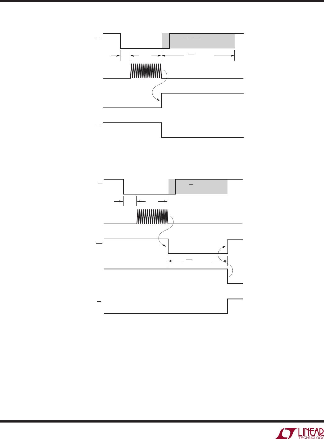
Simplified Power On/Off Sequence
Figure 1 shows a simplified LTC2950-1 power on and power
off sequence. A high to low transition on PB (t
1
) initiates
the power on sequence. This diagram does not show any
bounce on PB. In order to assert the enable output, the
PB pin must stay low continuously (PB high resets timers)
for a time controlled by the default 32ms and the external
ONT capacitor (t
2
–t
1
). Once EN goes high (t
2
), an internal
512ms blanking timer is started. This blanking timer is
designed to give sufficient time for the DC/DC converter
to reach its final voltage, and to allow the µP enough time
to perform power on tasks.
The KILL pin must be pulled high within 512ms of the EN
pin going high. Failure to do so results in the EN pin going
low 512ms after it went high. (EN = low, see Figure 2).
Note that the LTC2950 does not sample KILL and PB until
after the 512ms internal timer has expired. The reason PB
is ignored is to ensure that the system is not forced off
while powering on. Once the 512ms timer expires (t
4
), the
release of the PB pin is then debounced with an internal
32ms timer. The system has now properly powered on
and the LTC2950 monitors PB and KILL (for a turnoff
command) while consuming only 6µA of supply current.
A high to low transition on PB (t
5
) initiates the power off
sequence. PB must stay low continuously (PB high resets
debounce timer) for a period controlled by the default 32ms
and the external OFFT capacitor (t
6
–t
5
). At the completion
of the OFFT timing (t
6
), an interrupt (INT) is set, signifying
that EN will be switched low in 1024ms. Once a system
has finished performing its power down operations, it
can set KILL low (t
7
) and thus immediately set EN low),
terminating the internal 1024ms timer. The release of the
PB pin is then debounced with an internal 32ms timer.
The system is now in its reset state: where the LTC2950
is in low power mode (6µA). PB is monitored for a high
to low transition.
applicaTions inForMaTion