Automotive High Current LED Controller
A6265
14
Allegro MicroSystems, LLC
115 Northeast Cutoff
Worcester, Massachusetts 01615-0036 U.S.A.
1.508.853.5000; www.allegromicro.com
This defines the minimum peak switch current as set by the
switch current sense resistor.
The current rating for the inductor should be greater, by some
margin, than the peak value above, I
L(PK)
. When selecting an
inductor from manufacturers datasheets, there are two current
levels usually defined, the smallest value being the figure to work
with:
• Saturation level, where the inductance value typically drops by
10%, or
• Temperature rise, where the part experiences a certain rise in
temperature at full rated current. This parameter can be defined
between a 20°C and 50°C rise in temperature. It is important to
understand how manufacturers define the maximum operating
temperature, because this can often incorporate the self-heating
temperature rise.
In most cases the limiting current is usually the saturation value.
To improve efficiency, the inductor should also have low winding
resistance, typically < 50 m, and the core material will usually
be ferrite, with low losses at the oscillator frequency.
Recommended inductor manufacturers/series are:
• Coilcraft/ MSS1278T
• TDK/ SLF12575 type H
Diode The diode should have a low forward voltage, to reduce
conduction losses, and a low capacitance, to reduce switching
losses. Schottky diodes can provide both these features if care-
fully selected. The forward voltage drop is a natural advantage
for Schottky diodes and reduces as the current rating increases.
However, as the current rating increases, the diode capacitance
also increases so the optimum selection is usually the lowest cur-
rent rating above the required maximum, in this case I
L(PK)
.
Switch Current Sense Resistor (RSS) Neither the absolute
value of the switch current nor the accuracy of the measurement
is important, because the regulator will continuously adjust the
switch current, within a closed loop, to provide sufficient energy
for the output. For maximum accuracy the switch sense resistor
value should be chosen to maximize the differential signal seen
by the sense amplifier. The input limit of the sense amplifier,
V
IDS
, and the maximum switch current, I
S
(max), therefore define
the maximum value of the sense resistor as:
R
SS
= V
IDS
/ I
S
(max) (22)
Where I
S
(max) is the maximum switch current and should be set
above the maximum inductor current, I
L(PK)
.
This represents the maximum measurable value of the switch
(and inductor) current; however, the peak switch current will
always be less than this, set by the control circuit, depending on
the input voltage and the required load conditions. Because the
switch current control is within a closed loop, it is possible to
reduce the value of the sense resistor to reduce its power dissipa-
tion. However this will reduce the accuracy of the regulated LED
current.
In Boost mode, the power loss in the switch sense resistor is
worse at the lowest input voltage:
P
LOSS
= (V
LED
[V
LED
– V
IN
(min)] / V
IN
(min)
2
) × R
SS
× I
2
LED
(23)
In Buck Boost mode, the power loss in the switch sense resistor
is worse at the lowest input voltage:
P
LOSS
= (V
LED
/ V
IN
(min))(V
LED
+ V
IN
(min)) × R
SS
× I
2
LED
(24)
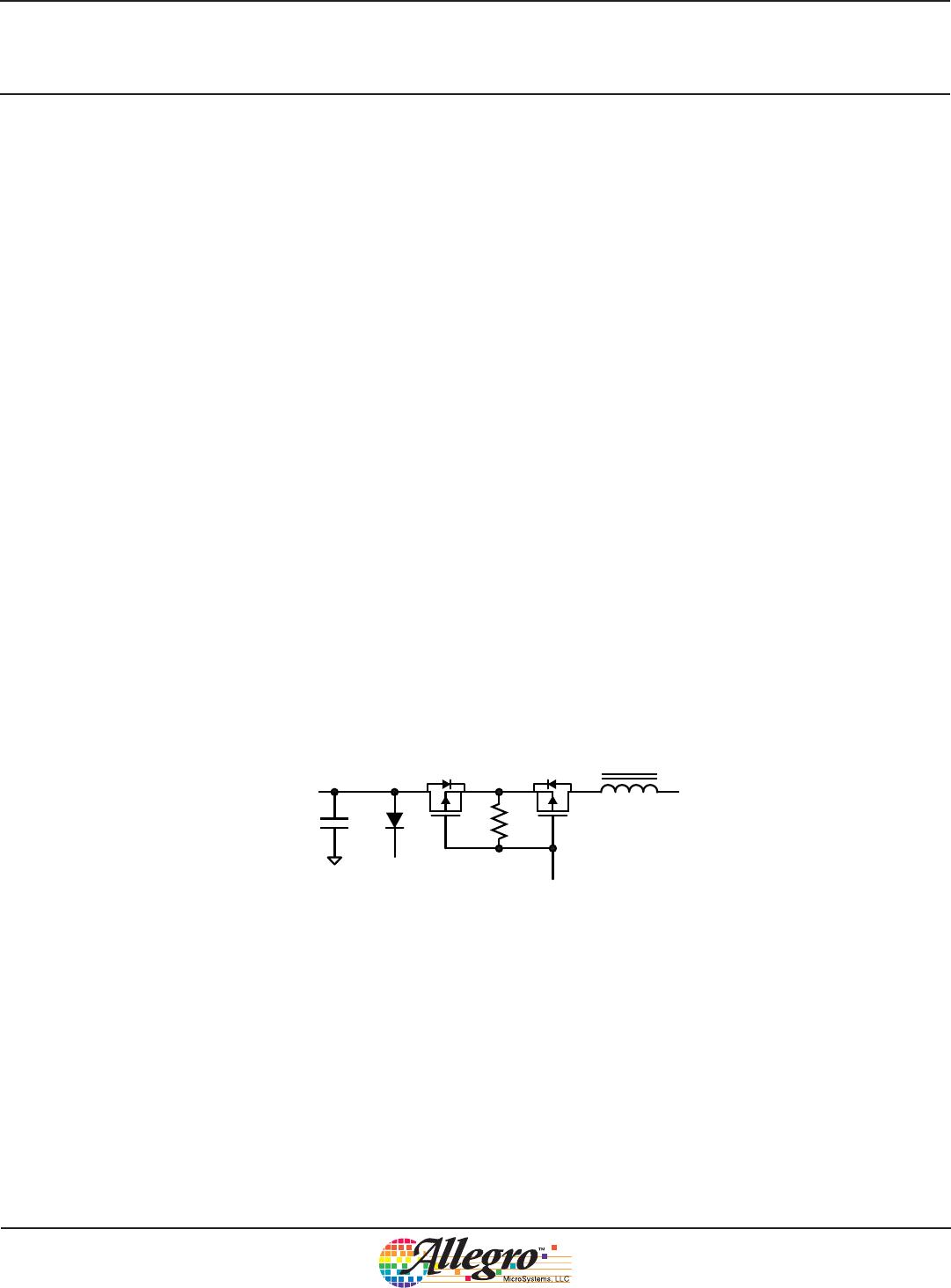
External Switch MOSFET A logic-level N-channel MOSFET
is used as the switch for the DC-to-DC converter. In the boost
configuration the voltage at the drain of the MOSFET is equal
to the maximum voltage across the string of LEDs. In the
buck-boost configuration the output voltage is referenced to
the positive supply. This means that the voltage at the drain of
the MOSFET will reach a voltage equal to the sum of the LED
voltage and the supply voltage. Under load dump conditions,
up to 90 V may be present on this node. In this case the external
MOSFET should therefore be rated at greater than 100 V.
The peak switch current is defined by the maximum inductor cur-
rent, I
L(PK)
. However in most cases the MOSFET will be chosen
by selecting low on-resistance, which usually results in a current
rating of several times the required peak current.
In addition to minimizing cost, the choice of MOSFET should
consider both the on-resistance and the total gate charge. The
total gate charge will determine the average current required from
the internal regulator and thus the power dissipation.